- DL manuals
- Yamaha
- Amplifier
- DSP-AX2
- Service Manual
Yamaha DSP-AX2 Service Manual
DSP-AX2
DSP-AX2
AV AMPLIFIER
1 0 0 7 2 9
This manual has been provided for the use of authorized YAMAHA Retailers and their service personnel.
It has been assumed that basic service procedures inherent to the industry, and more specifically YAMAHA Products, are already
known and understood by the users, and have therefore not been restated.
WARNING:
Failure to follow appropriate service and safety procedures when servicing this product may result in personal
injury, destruction of expensive components, and failure of the product to perform as specified. For these
reasons, we advise all YAMAHA product owners that any service required should be performed by an
authorized YAMAHA Retailer or the appointed service representative.
IMPORTANT:
The presentation or sale of this manual to any individual or firm does not constitute authorization, certification
or recognition of any applicable technical capabilities, or establish a principle-agent relationship of any
form.
The data provided is believed to be accurate and applicable to the unit(s) indicated on the cover. The research, engineering, and
service departments of YAMAHA are continually striving to improve YAMAHA products. Modifications are, therefore,
inevitable and specifications are subject to change without notice or obligation to retrofit. Should any discrepancy appear to exist,
please contact the distributor's Service Division.
WARNING:
Static discharges can destroy expensive components. Discharge any static electricity your body may have
accumulated by grounding yourself to the ground buss in the unit (heavy gauge black wires connect to this
buss).
IMPORTANT:
Turn the unit OFF during disassembly and part replacement. Recheck all work before you apply power to the
unit.
IMPORTANT NOTICE
DSP-AX2
SERVICE MANUAL
■ CONTENTS
TO SERVICE PERSONNEL ........................................... 1
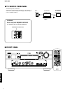
FRONT PANEL ............................................................... 1
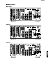
REAR PANELS ............................................................... 2
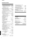
SPECIFICATIONS ..................................................... 4 – 5
INTERNAL VIEW ............................................................ 6
DISASSEMBLY PROCEDURES .................................... 6
SELF DIAGNOSIS FUNCTION ............................... 7 – 25
AMP CHECK ................................................................. 26
IC DATA ................................................................ 27 – 40
DISPLAY DATA .................................................... 41 – 42
PIN CONNECTION DIAGRAM ..................................... 43
BLOCK DIAGRAM ................................................ 44 – 47
PRINTED CIRCUIT BOARD ................................. 48 – 71
SCHEMATIC DIAGRAM ....................................... 72 – 78
PARTS LIST ........................................................ 79 – 102
Summary of DSP-AX2
Page 1
Dsp-ax2 dsp-ax2 av amplifier 1 0 0 7 2 9 this manual has been provided for the use of authorized yamaha retailers and their service personnel. It has been assumed that basic service procedures inherent to the industry, and more specifically yamaha products, are already known and understood by the us...
Page 2
Dsp-ax2 dsp-ax2 ■ to service personnel critical components information components having special characteristics are marked z and must be replaced with parts having specifications equal to those originally installed. Ac leakage tester or equivalent equipment under test insulating table wall outlet 1...
Page 3
Dsp-ax2 dsp-ax2 2 ▼ r, t models ■ rear panels 240 ▼ b model ▼ g model.
Page 4
Dsp-ax2 dsp-ax2 3 ■ audio section minimum rms output power per channel main, 20hz to 20khz, 0.02% thd, 8 Ω . . . 100w+100w center, 20hz to 20khz, 0.02% thd, 8 Ω . . . . . . 100w rear, 20hz to 20khz, 0.02% thd, 8 Ω . . . 100w+100w rear center, 20hz to 20khz, 0.02% thd, 8 Ω . . . . . . . . . . . . . ....
Page 5
Dsp-ax2 dsp-ax2 4 ■ general power supply b, g models . . . . . . . . . . . . . . . . . . . . . . . Ac 230v, 50hz r, t models . . . . . . . . . . . Ac 110/120/220/240v, 50/60hz power consumption . . . . . . . . . . . . . . . . . . . . . . . . . . . 480w maximum power consumption (r, t models only) . ...
Page 6
Dsp-ax2 dsp-ax2 5 ● set menu table no. Set menu preset value setting ranges 1. Speaker set 1a center speaker large large/small/none 1b main speaker large large/small 1c rear l/r speaker large large/small/none 1d rear ct speaker large large/small/none 1e lfe/bass out both subwoofer/main/both 1f front...
Page 7
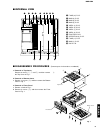
Dsp-ax2 dsp-ax2 6 ■ internal view ■ disassembly procedures (remove parts in the order as numbered.) 1. Removal of top cover remove 8 screws ( q , w and e ) and then remove the top cover in fig. 1. 2. Removal of bottom cover a. Remove 13 screws ( r ) and then remove the bottom cover in fig. 1. 3. Rem...
Page 8
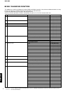
Dsp-ax2 dsp-ax2 7 ■ self diagnosis function this product has a built-in self diagnosis function (diag) to facilitate inspection, measurement and determination of a faulty item, if any. There are 13 diag menu items each of which has sub-menu items. Listed in the table below are menu items and sub-men...
Page 9
Dsp-ax2 dsp-ax2 8 no. 11 12 13 diag menu if status dsp ram check sum/ver/port sub-menu 16. Yss2 17. Yss3 dsp ram check 1. Version 2. Checksum (all/prog) 3. Checksum (232c/maker) 4. Port (check of port settings for judging micrprocessor function) remote control code (key) --------- --------- 7a---0a ...
Page 10
Dsp-ax2 dsp-ax2 9 1.Dsp thr 8.Rs232c 2.Hp route 9.Preset 3.Ram thr 10.Ad data 4.Pro logic 11.Status 5.Sp set 12.Dsp ram 6.Disp check 13.Ver sum 7.Manl test diagnostic menu ● display at the start of diag the diagnostic menu appears on the monitor screen. (it remains on display until it is canceled.) ...
Page 11
Dsp-ax2 dsp-ax2 10 in the case where the protection function works after diag has been started and the power is turned off ; when the protection function (*2) works, the history of the protection function appears on display and the power turns off. Repair the faulty parts according to the displayed ...
Page 12
Dsp-ax2 dsp-ax2 11 ● operation procedure of diag menu and sub-menu there are no.1 to no.13 menu items and some sub-menu items as well. Diag menu selection main unit: dsp program selector (forward/reverse) remote control unit: cursor h (forward)/ g (reverse) key sub-menu selection main unit: effect k...
Page 13
Dsp-ax2 dsp-ax2 12 1. Dsp through there are 3 sub menu items (analog byps, dsp 0db, full bit). Details of diag menu note: (sdoxx) represents a terminal name of ac3d3. The shaded square ( ) means that the element included in it does not operate. Analog byps [remote control code: 7a—90(prg 9)] • the i...
Page 14
Dsp-ax2 dsp-ax2 13 dsp 0db [remote control code: 7a—91 (prg 10)] • the input signal is automatically identified and switched in the priority order of dts ➝ dolby digital ➝ pcm audio ➝ analog (a/d) according to the signal detection. • l/r, c/rc, fl/fr, rl/rr and swfr signals are output through dsp (s...
Page 15
Dsp-ax2 dsp-ax2 14 full bit [remote control code: 7a—92 (prg11)] • the head margin is unused and the digital data is output in full bit. • the same applies as “dsp 0db” except that the digital data is output in full bit at d/a but swfr is not output in full bit. 2. Hp route (headphone route) there a...
Page 16
Dsp-ax2 dsp-ax2 15 full bit [remote control code: 7a—10 (tuner preset +)] • the head margin is unused and the digital data is output in full bit. • the same applies as “0db” except that the digital data is output in full bit at d/a but swfr is not output in full bit. 2. Hp route full bit (in the cas...
Page 17
Dsp-ax2 dsp-ax2 16 3. Ram through the input data is automatically identified and switched in the priority order of dts ➝ dolby digital ➝ pcm audio ➝ analog (a/d) according to the signal detection. The main l/r uses the analog through method when analog signals are input and the dsp through method wh...
Page 18
Dsp-ax2 dsp-ax2 17 swfr rl rr fl fr c rc l r filter df1704 filter df1704 filter df1704 d/a pcm1704 d/a pcm1704 d/a pcm1704 codec (d/a) ak4527 l/r l/r c sdoa0 sdob0 sdob1 sdob2 sdob3 codec (a/d) ak4527 dir dolby pro logic decoder main dsp (decoder) sub dsp digital analog ac3d3 yss928 c/s l/r 4m dram ...
Page 19
Dsp-ax2 dsp-ax2 18 the analog switch settings for each sub-menu are as shown in the table below. Sub-menu 1 main : small 0db 2 main : large -10 3 center : none 4 lfe/bass : main 5 front mix : 5ch 6 rear center : mute 7 rear l/r: mute center large large none small large large large rear large large l...
Page 20
Dsp-ax2 dsp-ax2 19 6. Display chk effect off 6. Display chk this program is used to check lighting of the fl display which changes as shown below according to operation of the sub-menu. The signals are processed using effect off. (the l/r signals are output using analog main bypass set- ting.) the v...
Page 21
Dsp-ax2 dsp-ax2 20 8. Rs-232c txd/rxd data:xx 8. Rs-232c hard flow :xx 7. Manual test all rxd rts cts txd 1 2 3 6 7 8 9 4 5 7. Manual test the test noise is output by the noise generator with a built-in dsp from the channels specified by the sub-menu. There are ten sub-menu items. All [remote contro...
Page 22
Dsp-ax2 dsp-ax2 21 9. Preset this menu reserves and inhibits initialization of the back-up ram (parameter, set menu contents, etc. For the sound field program). The signals are processed using effect off. (the l/r signals are output using analog main bypass set- ting.) reserved (initialization reser...
Page 23
Dsp-ax2 dsp-ax2 22 thm prd prv 028 006 009 the above figures are ex- amples for reference. Thm/prd/prv [remote control code: 7a—0b (cd skip –)] (detection of the temperature of the heat sink and protection function) thm: detection of the temperature of the heat sink (normal value: 6~40) 0.3v~ 2.0v (...
Page 24
Dsp-ax2 dsp-ax2 23 11. If status (input function status) using this menu, the status data is displayed in the hexadecimal notation one after another. During signal processing, the status before execution of this menu is maintained. To convert the analog input to the digital input, use the following ...
Page 25
Dsp-ax2 dsp-ax2 24 bit7 mute requested bit6 dts flashing (red) bit5 ex sound field being processed bit4 full mute (on: 1) bit3 – bit2 through & bypass (*2) bit1 – bit0 dts analog mute 5th byte indicates the information on the signal processing status. (*2): in the case of digital signals other than ...
Page 26
Dsp-ax2 dsp-ax2 25 13. Sum/ver /port there are four sub-menu items. Indicates the program version, checksum, specified port of the microprocessor (ic526 of the function circuit board). The checksum is obtained by adding data for every 16 bits for each program area and expressing the result as a 4-fi...
Page 27
Dsp-ax2 dsp-ax2 26 q93 q89 q86 q82 q79 q75 q72 q68 q65 q61 q58 q54 100 – 300 mv (l) 100 – 300 mv (r) 100 – 300 mv (c) 100 – 300 mv (rl) 100 – 300 mv (rr) 100 – 300 mv (rc) ● test point 100 – 350 mv (fl) 100 – 350 mv (fr) q362 q359 q357 q354 ic355 ic356 ic352 ic354 ic353 r385 r376 ■ amp check ● confi...
Page 28
Dsp-ax2 dsp-ax2 27 ■ ic data ic526 : m30802sgp (function p.C.B.) 16 bit µ -com (cpu) 109 110 111 112 113 114 115 116 117 118 119 120 121 122 123 124 125 126 127 128 129 130 131 132 133 134 135 136 137 138 139 140 141 142 143 144 1 2 3 4 5 6 7 8 9 10 11 12 13 14 15 16 17 18 19 20 21 22 23 24 25 26 27...
Page 29
Dsp-ax2 dsp-ax2 28 ic526 : m30802sgp (function p.C.B.) 16 bit µ -com (cpu) no. Port name function power on power off backup 1 txd4 txdr 232c transmission data o ol ol 2 p95 rts 232c rts out i/o ol ol 3 cts4 cts 232c cts input i i ol 4 da0 fan fan control i i ol 5 p92 sdtn sdt for non audio so ol ol ...
Page 30
Dsp-ax2 dsp-ax2 29 ic526 : m30802sgp (function p.C.B.) 16 bit µ -com (cpu) no. Port name function power on power off backup 56 p133 /bec bass extension control o ol ol 57 vss vss ground --- --- --- 58 p132 /z2mt zone2 mute o ol ol 59 vcc vcc + 5v --- --- --- 60 p131 /hpmt head phone mute o ol ol 61 ...
Page 31
Dsp-ax2 dsp-ax2 30 ic526 : m30802sgp (function p.C.B.) 16 bit µ -com (cpu) no. Port name function power on power off backup 111 d6 d6 data bus --- --- --- 112 d5 d5 data bus --- --- --- 113 d4 d4 data bus --- --- --- 114 p114 /mlv main level select (0/-10db) o ol ol 115 p113 pry power relay o ol ol ...
Page 32
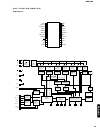
Dsp-ax2 dsp-ax2 31 ic501 : yss928 (dsp p.C.B.) ac3d3 120 11 118 117 116 11 114 113 112 111 110 109 108 59 58 57 56 55 54 53 52 51 50 49 48 47 46 45 44 43 42 41 78 77 80 79 76 75 74 73 72 71 70 69 68 67 66 65 64 63 62 61 60 13 107 14 106 15 105 16 104 17 103 18 102 19 101 20 100 99 98 97 96 95 94 93 ...
Page 33
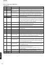
Dsp-ax2 dsp-ax2 32 no. Name i/o function 1 xo o crystal oscillator connecting terminal 2 xi i crystal oscillator connecting terminal (24.576mhz ) 3 seli1 i+ built-in selector input 1 (axd) 4 seli0 i+ built-in selector input 0 (gnd) 5 seloa o+ built-in selector output a (isel) 6 selob o+ built-in sel...
Page 34
Dsp-ax2 dsp-ax2 33 no. Name i/o function 56 sdwcki1 i+ word clock input terminal for sdib, sdob interface (unconnected) 57 sdbcki1 i+ bit clock input terminal for sdib, sdob interface (unconnected) 58 vss ground terminal 59 sdob3 o pcm output terminal from sub dsp 60 sdob2 o pcm output terminal from...
Page 35
Dsp-ax2 dsp-ax2 34 no. Name i/o function 111 rama5 o sub dsp: external memory address terminal 5 112 rama2 o sub dsp: external memory address terminal 2 113 seli13 i+ built-in selector input 13 (ac3rf) 114 seli12 i+ built-in selector input 12 (cxe) 115 seli11 i+ built-in selector input 11 (unconnect...
Page 36
Dsp-ax2 dsp-ax2 35 ic503 : pm4007a (dsp p.C.B.) ac-3 rf demodulator gnd vdd muti c1f0 c1f1 c2f0 c2f1 ti8 d asel da in d a out d asy o vld y ti5 mut o pddis ti4 pdo tdo trp tck tldb ti3 ti2 v out vin ti1 gnd vdd db0 80 79 78 77 76 75 74 73 72 71 70 69 68 67 66 65 64 63 62 61 60 59 58 57 56 55 54 53 5...
Page 37
Dsp-ax2 dsp-ax2 36 ic503 : pm4007a (dsp p.C.B.) ac-3 rf demodulator no. Name i/o function 30 a6 o external ram address output. Address 6 31 a7 o external ram address output. Address 7 32 gnd ground terminal (0v) 33 vdd +5v power supply 34 a12 o external ram address output. Address 12 35 a14 o extern...
Page 38
Dsp-ax2 dsp-ax2 37 ic503 : pm4007a (dsp p.C.B.) ac-3 rf demodulator no. Name i/o function 81 avdd +5v power supply for analog comparator 82 cpin i analog comparator input, positive side (non-reverse side: qpsk input) 83 cmin i analog comparator input, negative side (reverse side) 84 agnd ground term...
Page 39
Dsp-ax2 dsp-ax2 38 ic610 : lc74781-9798 (video p.C.B.) superimpose horizontal display position detection horizontal direction character size register horizontal size counter synchronous separation character output dot clock generator synchronous distinction complex synchronous signal separation cont...
Page 40
Dsp-ax2 dsp-ax2 39 symbol vss1 xtal in xtal out ctrl1 blank osc in osc out chara /cs sclk sin vdd2 cv out nc cv in vdd1 syn in sep c sep out sep in ctrl2 ctrl3 /rst vdd1 pin no. 1 2 3 4 5 6 7 8 9 10 11 12 13 14 15 16 17 18 19 20 21 22 23 24 function connection to gnd (digital system ground terminal)...
Page 41
Dsp-ax2 dsp-ax2 40 no. Port name function power on power off backup 1 vss vss ground --- --- --- 2 data data serial data input i i i 3 clock clock shift clock of data (rise edge trigger) i i i 4 lck lck latch clock of data (rise edge trigger) i i i 5 q0 via video input a o ol ol 6 q1 vib video input...
Page 42
Dsp-ax2 dsp-ax2 41 ■ display data v901 : 32-bt-07g (v6291200) q ^9 &0 pattern area 138 ● pin connection ● grid assignment note 1) f1, f2 ......... Filament 2) np .............. No pin 3) p1a~p35a, p1b~p35b ..... Datum line 4) 1ga~16ga, 1gb~16gb .............. Grid 5) ic ................ Internal con...
Page 43
Dsp-ax2 dsp-ax2 42 ● anode connection.
Page 44
Dsp-ax2 dsp-ax2 43 ● ics njm79m05fa njm79m12fa pq025ez5mzp njm7805fa njm7812fa njm78m05fa 1:common 2:input 3:output 3 2 1 1: output 2: common 3: input 3 2 1 tc74hcu04ap tc4066bp µ pc4570ha m5220l njm2068l-d njm4556al tc74hc4051ap tc74hc4053ap 1 7 14 njm2068md-t1 njm2904m-t1 µ pc4570g2 tk15420m 1 9 1...
Page 45
A b c d e f g h 1 2 3 4 5 6 dsp-ax2 e-45/j-43 ■ block diagram phono (l/r) cd (l/r) dvd (l/r) d-tv/ld (l/r) cable (l/r) a udio sat (l/r) md/tape in (l/r) cd-r in (l/r) vcr in (l/r) vcr 2/dvr in (l/r) video aux (l/r) md/tape out (l/r) cd-r out (l/r) vcr 1 out (l/r) vcr 2/dvr out (l/r) main (l/r) cente...
Page 46
A b c d e f g h 1 2 3 4 5 6 dsp-ax2 ■ block diagram e-46/j-44 dvd d-tv/ld cable sat vcr 1 vcr 2 dvr video aux dvd d-tv/ld cable sat vcr 1 vcr 2 dvr video aux c-input selector ic602 y-input selector ic603 c-recout selector ic604 y-recout selector ic605 ic609 input selector ic702 recout selector ic703...
Page 47
A b c d e f g h 1 2 3 4 5 6 dsp-ax2 ■ printed circuit board (foil side) e-49/j-47 point q (pin 1 of ic501) v : 2v/div, h : 50 nsec/div dc, 1 : 1 probe 0v 1 10 20 11 1 10 20 11 1 10 20 11 1 7 14 8 1 14 28 15 1 14 28 15 1 11 33 23 22 12 34 44 1 14 15 28 81 100 50 31 30 1 51 80 1 8 5 4 1 8 5 4 1 40 41 ...
Page 48
A b c d e f g h 1 2 3 4 5 6 dsp-ax2 ■ printed circuit board (foil side) e-50/j-48 1 36 37 72 73 108 109 144 1 24 48 25 1 15 16 30 1 15 16 30 1 15 16 30 1 15 16 30 1 15 16 30 16 30 1 15 1 8 5 4 1 8 5 4 1 8 5 4 1 8 5 4 1 8 5 4 1 8 5 4 1 8 5 4 1 8 5 4 1 8 5 4 1 8 5 4 1 8 5 4 1 8 5 4 1 16 9 8 16 9 1 8 1...
Page 49
A b c d e f g h 1 2 3 4 5 6 dsp-ax2 ■ printed circuit board (foil side) e-53/j-51 g only b, g only j, r, t only g only function p.C.B. (surface mount device) ref. No. Location d504 e3 d505 e3 d506 e4 d507 e4 ● semiconductor location ref. No. Location q510 c4 q511 b4 q512 c4 q513 b4 q515 d3 q517 d3 q...
Page 50
A b c d e f g h 1 2 3 4 5 6 dsp-ax2 ■ printed circuit board (foil side) e-54/j-52 s-video dvd d-tv/ld cable sat in out in out monitor out vcr 1 vcr 2/dvr i/e sdtn sckn axv axy axc vsy ceb ces +5v -5v axe from : function r/z vrb vic via /vr1 vse -5v +5v from : video (2) vrc vra vib /vr2 mon vg axv +5...
Page 51
A b c d e f g h 1 2 3 4 5 6 dsp-ax2 ■ printed circuit board (foil side) e-57/j-55 video monitor out out in out in sat cable d-tv/ld dvd vcr 1 vcr 2/dvr r/z vrb vic via /vr1 vsel -5v +5v from : video (1) vrc vra vib /vr2 mon vg axv g g g from : f amp (1) 1 8 9 16 1 8 9 16 g only video (2) p.C.B. (lea...
Page 52
A b c d e f g h 1 2 3 4 5 6 dsp-ax2 ■ printed circuit board (foil side) e-58/j-56 main out l/r main in l/r rear l/r front l/r mon out y p b /c b p r /c r d-tv/ld y p b /c b p r /c r dvd y p b /c b p r /c r pre out/main in rear center/center subwoofer l/r component video com1 cmp0 -5v +5v from : vide...
Page 53
A b c d e f g h 1 2 3 4 5 6 dsp-ax2 ■ printed circuit board (foil side) e-61/j-59 input input mode q w rm+ cem0 /flr key1 +5m psw mg rm- cem1 sckn sdtm key0 rem +5v from : function to : f amp (1) w901 #901 fl2 fl1 vp flg psw +5m to : operation (3) mg key0 key1 from : operation (6) operation (1) p.C....
Page 54
A b c d e f g h 1 2 3 4 5 6 dsp-ax2 ■ printed circuit board (foil side) e-62/j-60 1 8 1 9 8 1 1 14 8 7 bass treble rec out dsp program reb rec mg -12 tor e tol hpr e hpmt rea +5m /bec +12 tir til e hpl /hpi from : function /hpi hpl hpe hpe hpr from : operation (8) operation (2) p.C.B. Optical l r vi...
Page 55
A b c d e f g h 1 2 3 4 5 6 dsp-ax2 ■ printed circuit board (foil side) e-65/j-63 q93 q89 q86 q82 q79 q75 q72 q68 q65 q61 q58 q54 r,t,b,g only r,t,b,g only l r c rl e pr o sp a spe ldo e e rc rr fpri pri spb lc from : function to : f amp (1) w8 #18 flg vp +b2 e e e sp a- sp a+ rre rr rl rle spe+ spe...
Page 56
A b c d e f g h 1 2 3 4 5 6 dsp-ax2 ■ printed circuit board (foil side) e-66/j-64 be be re re bl re w5 bl w6 be w7 fr om : po wer transformer to : main (1) ach ach ach ach ac ac t o : main (3) acl acl acl acl ac ac t o : main (3) main (2) p.C.B. W12 w11 ● r, t, b, g models ach ach ach ach ac ac t o ...
Page 57
A b c d e f g h 1 2 3 4 5 6 dsp-ax2 ■ printed circuit board (foil side) e-69/j-67 vi bl vi or bl or from : power transformer from : power transformer ye ye flg vp fl1 fl2 pr v -5v +5d2 +5d1 +5v -12 +12 from : operation (1) from : operation (1) thm fa n pri pr o fr e fl from : function fa m + fa n - ...
Page 58
A b c d e f g h 1 2 3 4 5 6 dsp-ax2 ■ printed circuit board (foil side) e-70/j-68 mg +mb pr y #311 w311 to : function be gy from : power transformer ac outlet f amp (2) p.C.B. ● b model gy be gy be ac in f amp (4) p.C.B. Mg +mb pr y #311 w311 to : function re vi br be from : power cord from : power ...
Page 59
A b c d e f g h 1 2 3 4 5 6 i j k l m n 7 8 9 10 dsp-ax2 ■ schematic diagram (dsp) * all voltage are measured with a 10m Ω /v dc electric volt meter. * components having special characteristics are marked z and must be replaced with parts having specifications equal to those originally installed. * ...
Page 60: Input Selector
A b c d e f g h 1 2 3 4 5 6 i j k l m n o 7 8 9 10 dsp-ax2 ■ schematic diagram (function) e-73/j-71 * all voltage are measured with a 10m Ω /v dc electric volt meter. * components having special characteristics are marked z and must be replaced with parts having specifications equal to those origina...
Page 61: Tone Control
A b c d e f g h 1 2 3 4 5 6 i j k l m n 7 8 9 10 dsp-ax2 ■ schematic diagram (operation) * all voltage are measured with a 10m Ω /v dc electric volt meter. * components having special characteristics are marked z and must be replaced with parts having specifications equal to those originally install...
Page 62: Relay Driver
A b c d e f g h 1 2 3 4 5 6 i j k l m n o 7 8 9 10 dsp-ax2 ■ schematic diagram (main) * all voltage are measured with a 10m Ω /v dc electric volt meter. * components having special characteristics are marked z and must be replaced with parts having specifications equal to those originally installed....
Page 63
A b c d e f g h 1 2 3 4 5 6 i j k 7 8 dsp-ax2 ■ schematic diagram (f amp) * all voltage are measured with a 10m Ω /v dc electric volt meter. * components having special characteristics are marked z and must be replaced with parts having specifications equal to those originally installed. * schematic...
Page 64: Superimpose
A b c d e f g h 1 2 3 4 5 6 i j k l 7 8 dsp-ax2 ■ schematic diagram (video 1/2) * all voltage are measured with a 10m Ω /v dc electric volt meter. * components having special characteristics are marked z and must be replaced with parts having specifications equal to those originally installed. * sch...
Page 65
A b c d e f g h 1 2 3 4 5 6 i j k 7 8 dsp-ax2 ■ schematic diagram (video 2/2) * all voltage are measured with a 10m Ω /v dc electric volt meter. * components having special characteristics are marked z and must be replaced with parts having specifications equal to those originally installed. * schem...
Page 66: Parts List
Dsp-ax2 dsp-ax2 79 abbreviations in this list are as follows : c.A.El.Chp : chip alumi. Electrolytic cap c.Ce : ceramic cap c.Ce.Array : ceramic cap array c.Ce.Chp : chip ceramic cap c.Ce.Ml : multilayer ceramic cap c.Ce.M.Chp : chip multilayer ceramic cap c.Ce.Safty : recognized ceramic cap c.Ce.Tu...
Page 67
Dsp-ax2 dsp-ax2 schm ref. Part no. Description new parts * schm ref. Part no. Description new parts * 80 p.C.B. Dsp * v6600100 p.C.B. Dsp(rt) * v6600200 p.C.B. Dsp(bg) cb501 v6022800 cn.Fbrlink 1p gp1fa551tz cb502 v6022800 cn.Fbrlink 1p gp1fa551tz cb503 v5478200 cn.Phot.Sn 1p gp1fa551rz cb504 v54782...
Page 68
Dsp-ax2 dsp-ax2 schm ref. Part no. Description new parts * schm ref. Part no. Description new parts * 81 p.C.B. Dsp c599 us135100 c.Ce.Chp 0.1uf 16v c6 us135100 c.Ce.Chp 0.1uf 16v c61 us135100 c.Ce.Chp 0.1uf 16v(rt) c62 us064100 c.Ce.M.Chp 0.01uf 50v(rt) c63 us061180 c.Ce.Chp 18pf 50v(rt) * c64 us06...
Page 69
Dsp-ax2 dsp-ax2 schm ref. Part no. Description new parts * schm ref. Part no. Description new parts * 82 p.C.B. Dsp c78 vi715100 c.Mylar 470pf 50v c79 uu147100 c.El 10uf 25v c710 uu147100 c.El 10uf 25v c711 uu147100 c.El 10uf 25v c712 uu147100 c.El 10uf 25v c713 vi715100 c.Mylar 470pf 50v c714 vi715...
Page 70
Dsp-ax2 dsp-ax2 schm ref. Part no. Description new parts * schm ref. Part no. Description new parts * 83 p.C.B. Dsp & f amp ic527 xf291a00 ic upc4570g2 l51 v2726500 coil 68uh l52 v2726500 coil 68uh l53 v2726500 coil 68uh l54 v2726500 coil 68uh l55 v2726500 coil 68uh l56 vt623200 fltr.Lc sbp‑4930(rt)...
Page 71
Dsp-ax2 dsp-ax2 schm ref. Part no. Description new parts * schm ref. Part no. Description new parts * 84 p.C.B. F amp c366 vs696700 c.Ce 33pf 500v c367 up652100 c.Pol 100pf 100v * c368 uu148100 c.El 100uf 25v c369 uu137470 c.El 47uf 16v c370 vr325000 c.Mylar 100pf 100v c371 ua654100 c.Mylar 0.01uf 5...
Page 72
Dsp-ax2 dsp-ax2 schm ref. Part no. Description new parts * schm ref. Part no. Description new parts * 85 p.C.B. F amp & main z r382 hv756220 r.Car.Fp 2.2kΩ 1/4w z r384 hv755100 r.Car.Fp 100Ω 1/4w z r385 hv755100 r.Car.Fp 100Ω 1/4w r389 hv754100 r.Car.Fp 10Ω 1/4w r390 hv753470 r.Car.Fp 4.7Ω 1/4w r391...
Page 73
Dsp-ax2 dsp-ax2 schm ref. Part no. Description new parts * schm ref. Part no. Description new parts * 86 p.C.B. Main c71 up652100 c.Pol 100pf 100v * c72 uu157330 c.El 33uf 35v c73 uu167100 c.El 10uf 50v c74 vk533900 c.Pp 100pf 200v * c75 uu148100 c.El 100uf 25v c76 vk533900 c.Pp 100pf 200v * c77 up6...
Page 74
Dsp-ax2 dsp-ax2 schm ref. Part no. Description new parts * schm ref. Part no. Description new parts * 87 p.C.B. Main d9 if004600 diode 1ss133 d10 vg440100 diode.Zenr mtzj12a 12v z * d11 vc398400 diode ma185 d12 if004600 diode 1ss133 d13 vg440100 diode.Zenr mtzj12a 12v z * d14 vc398400 diode ma185 d1...
Page 75
Dsp-ax2 dsp-ax2 schm ref. Part no. Description new parts * schm ref. Part no. Description new parts * 88 p.C.B. Main z q40 ve198700 tr 2sa1145 o,y z q41 ic224030 tr 2sc2240 gr,bl z q42 ic224030 tr 2sc2240 gr,bl z q43 ic224030 tr 2sc2240 gr,bl z q44 ic224030 tr 2sc2240 gr,bl z q45 ia1015i0 tr 2sa1015...
Page 76
Dsp-ax2 dsp-ax2 schm ref. Part no. Description new parts * schm ref. Part no. Description new parts * 89 p.C.B. Main & function z r138 hv755680 r.Car.Fp 680Ω 1/4w z r139 hv755100 r.Car.Fp 100Ω 1/4w z r141 hv755470 r.Car.Fp 470Ω 1/4w z r146 hv755470 r.Car.Fp 470Ω 1/4w z r150 hv756680 r.Car.Fp 6.8kΩ 1...
Page 77
Dsp-ax2 dsp-ax2 schm ref. Part no. Description new parts * schm ref. Part no. Description new parts * 90 p.C.B. Function cb512 vb858400 cn.Bs.Pin 5p cb513 vb858200 cn.Bs.Pin 3p cb515 vq047300 cn.Bs.Pin 12p cb516 vf982200 cn.Bs.Pin 14p cb517 vb858200 cn.Bs.Pin 3p c501 vd930900 c.Ce.Smi 0.1uf 25v c503...
Page 78
Dsp-ax2 dsp-ax2 schm ref. Part no. Description new parts * schm ref. Part no. Description new parts * 91 p.C.B. Function c622 us135100 c.Ce.Chp 0.1uf 16v c623 uu147100 c.El 10uf 25v c624 uu147100 c.El 10uf 25v c625 us135100 c.Ce.Chp 0.1uf 16v c626 us135100 c.Ce.Chp 0.1uf 16v c627 us135100 c.Ce.Chp 0...
Page 79
Dsp-ax2 dsp-ax2 schm ref. Part no. Description new parts * schm ref. Part no. Description new parts * 92 p.C.B. Function & video ic519 xw173a00 ic cs3310‑ks ic520 xw173a00 ic cs3310‑ks ic521 xf291a00 ic upc4570g2 ic522 xp896a00 ic lc78213 ic523 xf291a00 ic upc4570g2 ic524 xf291a00 ic upc4570g2 ic525...
Page 80
Dsp-ax2 dsp-ax2 schm ref. Part no. Description new parts * schm ref. Part no. Description new parts * 93 p.C.B. Video c602 us062100 c.Ce.M.Chp 100pf 50v c603 us062100 c.Ce.M.Chp 100pf 50v c604 us062100 c.Ce.M.Chp 100pf 50v c605 us062100 c.Ce.M.Chp 100pf 50v c606 us062100 c.Ce.M.Chp 100pf 50v c607 us...
Page 81
Dsp-ax2 dsp-ax2 schm ref. Part no. Description new parts * schm ref. Part no. Description new parts * 94 p.C.B. Video & operation d605 if004600 diode 1ss133 d606 if004600 diode 1ss133 d607 if004600 diode 1ss133 d608 if004600 diode 1ss133 d609 if004600 diode 1ss133 d610 if004600 diode 1ss133 ic601 xw...
Page 82
95 96 dsp-ax2 p.C.B. Operation schm ref. Part no. Description new parts * schm ref. Part no. Description new parts * chip resistor rd350000 r.Car.Chp 0Ω 1/10w rd353100 r.Car.Chp 1Ω 1/10w rd353220 r.Car.Chp 2.2Ω 1/10w rd354330 r.Car.Chp 33Ω 1/10w rd354470 r.Car.Chp 47Ω 1/16w rd354680 r.Car.Chp 68Ω 1/...
Page 83
A b c d e f g h 1 2 3 4 5 6 dsp-ax2 ■ exploded view 97 98 4-12 4-10 4-8 4-10 4-2 4-6 4-6 4-4 5-13 5-1 5-7 5-7 5-9 5-6 5-6 5-7 5-5 4-1 85 123 2-1-13 2-1-25 2-1-21 2-1-11 2-1-28 2-1-17 2-1-6 2-1-4 2-1-24 2-1-26 2-1-15 2-1-18 2-1-16 2-1-26 2-1-5 2-1-27 2-1-23 2-1-22 2-1-25 2-1-3 2-1-28 1-8 1-5 1-15 1-1...
Page 84
Dsp-ax2 99 100 ■ mechanical parts ref. No. Part no. Description remarks markets new parts * ref. No. Part no. Description remarks markets new parts * * 1‑1 v6076700 front panel ti * 1‑1 v6066000 front panel bl * 1‑1 v6066100 front panel gd * 1‑3 v6065300 support/esc * 1‑4 v6066900 escutcheon/side r ...
Page 85
Dsp-ax2 101 102 ref. No. Part no. Description remarks markets new parts * ref. No. Part no. Description remarks markets new parts * 32 mf112100 flexible flat cable 12p 100mm p=1.25 * 33 v6684100 s flexible flat cable 15p 350mm p=1.25 * 34 mf111400 flexible flat cable 11p 400mm * 35 mf117140 flexible...
Page 86: Remote Control Transmitter
A b c d e f g h 1 2 3 4 5 6 dsp-ax2 remote control transmitter 81 82 83 84 85 86 87 88 89 90 91 92 93 94 95 96 97 98 99 100 p07 p06 p05 p04 p03 p02 p01 p00 p107 p106 p105 p104 p103 p102 p101 p100 p16 p13 p07 p06 p05 p04 p03 p02 p01 p00 p107 (ki.P.U) p106 (ki.P.U) p105 (ki.P.U) p104 (ki.P.U) p103 (p....
Page 87
Dsp-ax2 key no. 42 43 44 45 46 47 48 49 50 51 52 53 54 55 56 57 58 59 60 61 62 63 64 65 66 67 68 69 70 71 72 key name sw2 prg1 prg2 prg3 prg4 prg5 prg6 prg7 prg8 prg9 prg10 prg11 prg12 chp/index tv vol up tv vol down tv input tv mute ch up ch down mute effect vol up vol down sw3 on screen sleep leve...
Page 88
Dsp-ax2 key 6 7 8 9 10 11 12 13 14 15 16 17 18 19 20 key name power on standby a v-aux phono d-tv tuner md/tape cd-r cd cable sat vcr1 vcr2/dvr dvd 1 k6 k7 k6 k6 k6 k6 k6 k6 k6 k6 k6 k6 k6 k6 k6 k35 k35 k35 k35 k35 k35 md/tape cd-r cd vcr1 vcr2 dvd 2 k39 tv ― ― k9 k10 k11 k12 k13 k14 k15 k16 k17 k18...
Page 89: Dsp-Ax2
Dsp-ax2 parts list for carbon resistors 1/6w type part no. Hf45 7100 hf45 7110 hf85 7120 hf45 7130 hf45 7150 hf45 7180 hf45 7220 hf45 7240 hf85 7270 hf45 7300 hf45 7330 hf45 7360 hf45 7390 hf45 7470 hf45 7510 hf45 7560 hf45 7620 hf45 7680 hf45 7820 hf45 7910 hf45 8100 hf45 8110 hf45 8120 hf45 8150 h...

