Cadence CADENCE ORCAD FPGA SYSTEM PLANNER System Planner
D
A
TA
S
H
E
E
T
D
A
TA
S
H
E
E
T
The Cadence
®
OrCAD
®
FPGA System Planner addresses the
challenges that engineers encounter when designing large-
pin-count FPGAs on the PCB board—which includes creating
the initial pin assignment, integrating with the schematic, and
ensuring that the device is routable on the board. It delivers
a complete, scalable technology for FPGA-PCB co-design that
automates creation of optimum “device-rules-accurate” pin
assignment. By replacing manual, error-prone processes with
automatic pin assignment synthesis, this unique placement-
aware solution eliminates unnecessary physical design itera-
tions while shortening the time required to create optimum pin
assignment.
Cadence FPGA System Planner
technologies are available in the
following product offerings:
•
Cadence Allegro FPGA System
Planner L, XL, and GXL
•
Cadence Allegro FPGA System
Planner Two FPGA Option L
•
Cadence OrCAD FPGA System
Planner
CADEnCE OrCAD FPGA
SySTEm PlAnnEr
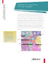
Figure 1: Color-coded map of the I/Os of a multi-bank FPGA with different types of configurable pins
User IO
Configurable
Clock
Capable
Differential
Power


