- DL manuals
- E2v
- Motherboard
- TSEV8308500
- User Manual
E2v TSEV8308500 User Manual
Summary of TSEV8308500
Page 1
Tsev8308500 evaluation board .............................................................................................. User guide.
Page 3
Tsev8308500 evaluation board user guide -i 0968d–bdc–01/09 e2v semiconductors sas 2009 table of contents section 1 overview............................................................................................... 1-1 1.1 description ................................................................
Page 4
-ii tsev8308500 evaluation board user guide 0968d–bdc–01/09 e2v semiconductors sas 2009 4.9 test bench description .............................................................................4-5 section 5 package description..............................................................................
Page 5: Section 1
Tsev8308500 evaluation board user guide 1-1 0968d–bdc–01/09 e2v semiconductors sas 2009 section 1 overview 1.1 description the tsev8308500 evaluation board (eb) is a prototype board which has been designed in order to facilitate the evaluation and the characterization of the ts8308500 device up to i...
Page 6
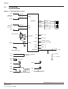
Overview 1-2 tsev8308500 evaluation board user guide 0968d–bdc–01/09 e2v semiconductors sas 2009 1.2 tsev8308500 evaluation board figure 1-1. Tsev8308500 block diagram clk clkb differential clock inputs z0 = 50 z0 = 50 clk clkb ts8308500 vin vinb differential clock inputs z0 = 50 z0 = 50 vin vinb ad...
Page 7
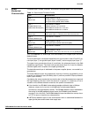
Overview tsev8308500 evaluation board user guide 1-3 0968d–bdc–01/09 1.3 board mechanical characteristics the board layer’s number, thickness, and functions are given below, from top to bottom. The tsev8308500 is a seven-layer pcb constituted by four copper layers and three dielectric layers. The fo...
Page 8
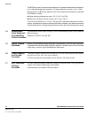
Overview 1-4 tsev8308500 evaluation board user guide 0968d–bdc–01/09 e2v semiconductors sas 2009 the bt/epoxy layer has been chosen because of its enhanced mechanical characteris- tics for elevated temperature operation. The typical dielectric constant is 4.5 at 1 mhz. More precisely, the bt/epoxy d...
Page 9: Section 2
Tsev8308500 evaluation board user guide 2-1 0968d–bdc–01/09 e2v semiconductors sas 2009 section 2 layout information 2.1 board the ts8308500 requires proper board layout for optimum full speed operation. The following explains the board layout recommendations and demonstrates how the evaluation boar...
Page 10
Layout information 2-2 tsev8308500 evaluation board user guide 0968d–bdc–01/09 e2v semiconductors sas 2009 2.4 power supplies the bottom metal layer 7 is dedicated to the power supply traces (v eea , v eed , v eet , v cc , v dd , v plusd ). The supply traces are approximately 6 mm wide in order to p...
Page 11: Section 3
Tsev8308500 evaluation board user guide 3-1 0968d–bdc–01/09 e2v semiconductors sas 2009 section 3 operating procedures and characteristics 3.1 introduction this section describes a typical single-ended configuration for analog inputs and clock inputs. The single-ended configuration is preferable, as...
Page 12
Operating procedures and characteristics 3-2 tsev8308500 evaluation board user guide 0968d–bdc–01/09 e2v semiconductors sas 2009 4. Connect the analog signal v in . The inverted phase clock input v inb may be left open (as on-board 50 Ω terminated). Use a low phase noise rf source. Full scale range ...
Page 13
Operating procedures and characteristics tsev8308500 evaluation board user guide 3-3 0968d–bdc–01/09 3.4 operating characteristics the power supplies denoted v cc , v eea , v eed and v plusd are dedicated for the ts8308500 adc. The power supplies denoted v eet , v dd are dedicated to the optional mc...
Page 14
Operating procedures and characteristics 3-4 tsev8308500 evaluation board user guide 0968d–bdc–01/09 e2v semiconductors sas 2009.
Page 15: Section 4
Tsev8308500 evaluation board user guide 4-1 0968d–bdc–01/09 e2v semiconductors sas 2009 section 4 application information 4.1 introduction for this section, refer also to the product specification application notes (ts8308500 datasheet). More particularly, refer to sections related to single-ended a...
Page 16
Application information 4-2 tsev8308500 evaluation board user guide 0968d–bdc–01/09 e2v semiconductors sas 2009 the v plusd positive supply voltage allows the adjustment of the output common mode level from -1.2v (v plusd = 0v for ecl output compatibility) to +1.2v (v plusd = 2.4v for lvds output co...
Page 17
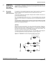
Application information tsev8308500 evaluation board user guide 4-3 0968d–bdc–01/09 4.7 temperature monitoring and data ready reset function one single pad is used for both drrb input command and die junction monitoring. The pad denomination is drrb/diod. Temperature monitoring and data ready contro...
Page 18
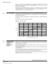
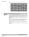
Application information 4-4 tsev8308500 evaluation board user guide 0968d–bdc–01/09 e2v semiconductors sas 2009 figure 4-3. Transistor vbe forward voltage versus junction temperature (i = 3 ma) 4.8 data ready output signal reset a subvis connector is provided for drrb command. The data ready signal ...
Page 19
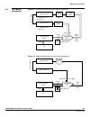
Application information tsev8308500 evaluation board user guide 4-5 0968d–bdc–01/09 4.9 test bench description figure 4-4. Differential analog and clock inputs configuration figure 4-5. Single-ended analog and clock input configuration signal generator signal generator -121 dbc/hz at 1 hz offset fro...
Page 20
Application information 4-6 tsev8308500 evaluation board user guide 0968d–bdc–01/09 e2v semiconductors sas 2009.
Page 21: Section 5
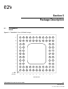
Tsev8308500 evaluation board user guide 5-1 0968d–bdc–01/09 e2v semiconductors sas 2009 section 5 package description 5.1 ts8308500gl pinout figure 5-1. Ts8308500gl pinout (cbga68 package) 1 2 3 4 5 6 7 8 9 10 11 vplusd vplusd nc b3b drb gnd gnd b4 b5 nc dvee gnd gnd b2 vplusd b3 dr b4b b5b vplusd b...
Page 22
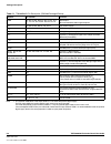
Package description 5-2 tsev8308500 evaluation board user guide 0968d–bdc–01/09 e2v semiconductors sas 2009 note: 1. The common mode level of the output buffers is 1.2v below the positive digital supply. For ecl compatibility the positive digital supply must be set at 0v (ground). For lvds compatibi...
Page 23
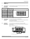
Package description tsev8308500 evaluation board user guide 5-3 0968d–bdc–01/09 5.2 thermal characteristics 5.2.1 thermal resistance from junction to ambient: rthja the following table lists the converter thermal performance parameters of the device itself, with no external heatsink added. 5.2.2 the...
Page 24
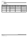
Package description 5-4 tsev8308500 evaluation board user guide 0968d–bdc–01/09 e2v semiconductors sas 2009 5.3 ordering information table 5-3. Ordering information part number package temperature range screening level comments tsx8308500gl cbga 68 ambient prototype prototype version ts8308500cgl cb...
Page 25: Section 6
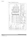
Tsev8308500 evaluation board user guide 6-1 0968d–bdc–01/09 e2v semiconductors sas 2009 section 6 schematics 6.1 tsev8308500 electrical schematics please, see the following figures..
Page 26
Schematics 6-2 tsev8308500 evaluation board user guide 0968d–bdc–01/09 e2v semiconductors sas 2009 figure 6-1. Tsev8308500 electrical schematic.
Page 27
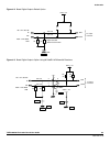
Schematics tsev8308500 evaluation board user guide 6-3 0968d–bdc–01/09 figure 6-2. Board digital outputs default option figure 6-3. Board digital outputs option using mc100el16 differential receivers vdd = -2v in inb out outb to output connector z0 = 50 z0 = 50 50 50 digital data 50 Ω differential t...
Page 28
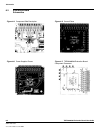
Schematics 6-4 tsev8308500 evaluation board user guide 0968d–bdc–01/09 e2v semiconductors sas 2009 6.2 evaluation board schematics figure 6-4. Component side description figure 6-5. Ground plane figure 6-6. Power supplies planes figure 6-7. Tsev8308500 evaluation board: component placement.
Page 29
0968d–bdc–01/09 e2v semiconductors sas 2009 whilst e2v has taken care to ensure the accuracy of the information contained herein it accepts no responsibility for the consequences of any use thereof and also reserves the right to change the specification of goods without notice. E2v accepts no liabil...

