- DL manuals
- Icom
- Transceiver
- IC-F33GS
- Service Manual
Icom IC-F33GS Service Manual
Summary of IC-F33GS
Page 1
S-14113iz-c1-q apr. 2007 vhf transceiver ic-f33gt ic-f33gs ic-f34gt ic-f34gs.
Page 2
This ser vice manual describes the latest ser vice information for the ic-f33gt/gs and ic-f34gt/gs vhf transceiver at the time of publication. Never connect the transceiver to an ac outlet or to a dc power supply that uses more than 8 v. This will ruin the transceiver. Do not expose the transceiver ...
Page 3
Contents section 1 specifications section 2 inside views section 3 disassembly instructions section 4 optional units installation section 5 circuit descripiton 5-1 receiver circuits. . . . . . . . . . . . . . . . . . . . . . . . . . . . . . . . . . . . . . . . . . . . . . . . . . . . . . . . 5-1 5-2...
Page 4: Section 1
1 - 1 section 1 specifications ■ general • frequency coverage : 136.000–174.000 mhz • mode : fm • type of emission : • number of conventional channels : 256 ch, 16 banks • antenna impedance : 50 Ω (nominal) • operating temperature range : –30˚c to +60˚c (–22˚f to +140˚f) [usa], [gen] –25˚c to +55˚c ...
Page 5: Section 2
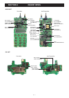
2 - 1 section 2 inside views tx mute switch (q501: unr9213j) pll ic (ic21: lmx2352tm) base band ic (ic14: ak2346) eeprom (ic10: 24lc64t-i/sn) cpu (ic22: hd64f2238btf13) r5 regulator (q25: 2sa1577) fm if ic (ic9: ta31136fn) af amplifier (ic15: ta7368f) apc amplifier (ic2: ta75s01f) if amplifier (q7: ...
Page 6: Section 3
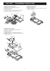
3 - 1 section 3 disassembly instruction • removing the chassis unit 1 unscrew 1 nut a, and remove 2 knobs b, c. 2 unscrew 2 screws d. 3 unscrew 2 screws e. 4 take off the chassis unit in the direction of the arrow. 5 unplug the connector f from the chassis unit. • removing the pa unit 1 unscrew 3 sc...
Page 7
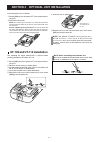
4 - 1 section 4 optional unit installation : s w o ll o f s a t i n u l a n o i t p o e h t ll a t s n i q e t a t o r ] l o v [ - t a b e h t e v o m e r d n a , f f o r e w o p e h t n r u t o t . K c a p y r e t w . R e v o c t i n u e h t e v o m e r : e t o n , t n e m u r t s n i t a fl r a li...
Page 8
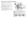
4 - 2 n e h w d e r i u q e r s i n o i t a c i f i d o m d r a o b c p g n i w o l l o f e h t : s 7 1 1 - t u r o 7 1 1 - t u , 5 0 1 - t u l a n o i t p o e h t g n il l a t s n i q e t a t o r ] l o v [ - t a b e h t e v o m e r d n a , f f o r e w o p e h t n r u t o t . K c a p y r e t w above...
Page 9: Section 5
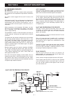
4 - 1 section 5 circuit description 1st if circuits the 1st if circuits consist of 1st mixer, 1st if fi lter and 1st if amplifi er, and converts the received signals into the 1st if signal, fi lters to remove unwanted signals and amplifi es. The rf signals from the bandpass filter are mixed with the...
Page 10
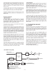
4 - 2 the filtered signals pass through the high-pass filter to sup- press unwanted harmonic components. The signals pass through (or bypass) scrambler and expander sections. The signals are amplified at the amplifier section in the base band ic (ic14). The output signals from ic14 (pin 20) pass thr...
Page 11
4 - 3 modulation circuit • voice signal the modulation circuit fm-modulates the vco oscillating signal with the af signals from the tx af circuit. The af signals from the microphone amplifier circuits are applied to the variable capacitor to change its reactance for fm modulation. The af signals fro...
Page 12
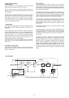
4 - 4 5-3 frequency synthesizer circuits vco a vco is an oscillator which its oscillation frequency is determined by the applied volatge. Shifting the oscillation frequency range in rx/tx, the vco generates both of the tx signal and 1st lo signals. There are two vcos; rx vco and tx vco. The rx vco g...
Page 13
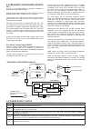
4 - 6 pin number port name description 13, 15, 16 cenc0– cenc2 output the ctcss/dtcs signals. 29 ref outputs the reference oscillator cor- recting voltage. The voltage is applied to the buffer amplifi er (ic24, pin 3) 30 plst outputs strobe signals to the pll ic (ic21, pin 16). 34 pmfm o u t p u t s...
Page 14: Section 6
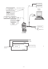
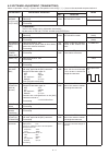
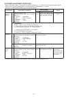
6 - 1 section 6 adjustment procedure equipment grade and range equipment grade and range dc power supply output voltage current capacity : 7.2 v dc : 5 a or more audio generator frequency range measuring range : 300–3000 hz : 1–500 mv fm deviation meter frequency range measuring range : dc–800 mhz :...
Page 15
6 - 2 fm deviation meter sinad meter speaker (8 ½) audio generator ac millivoltmeter to the antenna connector attenuator 20 db or 30 db rf power meter 0.1Ð10 w/50 ½ frequency counter standard signal generator 0.1 µv to 32 mv (Ð127 dbm to Ð17 dbm) caution! Do not transmit while an ssg is connected to...
Page 16
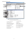
6 - 3 • cs-f33g adj's screen example q: transceiver's connection state w: reload adjustment data e: receive sensitivity measurement r: connected dc voltage measurement t: pll lock voltage measurement y: operating channel select u: rf output power i: fm modulation balance (narrow) o: fm deviation (na...
Page 17
6 - 4 adjustment adjustment condition measurement value unit location pll lock voltage [lv (rx lva)] [lv (tx lva)] 1 • operating channel : ch7 • receiving pc screen check the "lvin" item on the cs-f33g adj's screen. 3.5 v 3.5 v 2 • operating channel : ch7 • transmitting convenient: the pll lock volt...
Page 18
6 - 5 adjustment adjustment condition measurement value unit location rx sensitivity [bpf t1] [bpf t2] 1 • operating channel : ch5 • connect the ssg to the antenna connector and set as: frequency : 136.000 mhz level : 10 µv* (–87 dbm) modulation : 1 khz deviation : ±3.5 khz • receiving pc screen con...
Page 19: Section 7
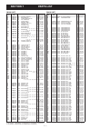
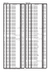
7 - 1 section 7 parts list m.=mounted side (t: mounted on the top side, b: mounted on the bottom side) [main unit] ref order description m. H/v no. No. Location ic2 1110002751 s.Ic ta75s01f (te85r,f) t 88.1/12.4 ic6 1110005340 s.Ic njm12902v-te1 b 55.4/23.8 ic8 1110005771 s.Ic s-80942cnmc-g9ct2g b 2...
Page 20
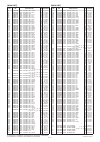
7 - 2 m.=mounted side (t: mounted on the top side, b: mounted on the bottom side) [main unit] ref order description m. H/v no. No. Location r92 7030005090 s.Res erj2gej 104 x (100 k) t 72.5/21.8 r93 7030005060 s.Res erj2gej 333 x (33 k) b 46.2/20.4 r94 7030010040 s.Res erj2gej-jpw t 72.3/29.6 r95 70...
Page 21
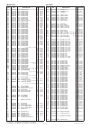
7 - 3 m.=mounted side (t: mounted on the top side, b: mounted on the bottom side) [main unit] ref order description m. H/v no. No. Location c25 4030017580 s.Cer ecj0ec1h060c b 96.6/34.6 c26 4030017460 s.Cer ecj0eb1e102k b 37.6/34.6 c27 4030017430 s.Cer ecj0ec1h101j b 96.7/39.8 c28 4030017370 s.Cer e...
Page 22
7 - 4 m.=mounted side (t: mounted on the top side, b: mounted on the bottom side) [main unit] ref order description m. H/v no. No. Location c347 4030017640 s.Cer ecj0ec1h150j b 27.4/36 c348 4030017400 s.Cer ecj0ec1h220j b 26.6/28 c349 4030017330 s.Cer ecj0ef1c104z b 26/31.5 c350 4030017330 s.Cer ecj...
Page 23
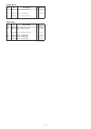
7 - 5 m.=mounted side (t: mounted on the top side, b: mounted on the bottom side) [fuse unit] ref order description m. H/v no. No. Location l901 6200006190 s.Col blm21pg300sn1d t 10.2/6 c901 4030017460 s.Cer ecj0eb1e102k t 6/6.6 j901 6910015881 cnr 9230b-1-02z141-pt1 s.=surface mount [ant unit] ref ...
Page 24: Section 8
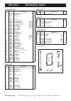
Screw abbreviations a, b0, bt: self-tapping ph: pan head zk: black ni-zu: nickel-zinc sus: stainless 8 - 1 section 8 mechanical parts [chassis parts] ref order description qty. No. No. J1 6910015910 ant connector 104 1 j2 6910015860 imsa-6277s-o2a-g 1 sp1 2510001061 k036na500-67 1 w1 8900009640 opc-...
Page 25
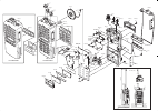
7 - 2 mp2(c) mp25(c) mp30(c) mp29(c) mp33(c) mp20(c) sp1(c) mp12(c) main unit mp28(c) mp37(c) mp42(c) mp4(m) ep7(m) ds3(m) mp3(m) mp21(c) mp22(c) mp34(c) mp28(c) s27(m) r315(m) mp28(c) pa unit fuse unit mp28(c) mp38(c) j901(f) j702(p) mp47(c) ant unit mp1(c) j1(c) mp36(c) mp35(c) mp17(c) mp8(c) mp31...
Page 26: Section 9
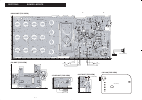
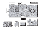
9 - 1 section 9 board layouts dc in (no patterns) • main unit (top view) • pa unit (top view) • fuse unit (top view) • ant unit (top view) • bc-160 (top view) 1 2 sp1 (chassis) j1 (chassis) j4 j3 clone sp mic micg afout vcc gnd j2 c17 4 2 c 6 3 c c37 2 4 c 3 4 c 1 5 c c55 c56 c57 2 6 c 6 6 c 9 6 c 0...
Page 27
9 - 2 h0 h5 h10 0 v 5 v 0 1 v 5 1 v s-14113ih-p2-q printed in japan © 2004−2007 icom inc. • main unit (bottom view) [monitor] [rotary selector] [vol] [ptt] [up] [down] • pa unit (bottom view) • fuse unit (bottom view) • ant unit (bottom view) • bc-160 (bottom view) mc1 j5 30 gnd pttin 1 +5v ptt out ...
Page 28: Section 10
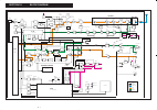
10 - 1 section 10 block diagram notes : contorol line common line tx line rx line data lime voltage line bpf 272.0-440.7 mhz d mute q502: 2sk3019 pre empha ic25: tc7s66fu sw lpf lpf ic6: njm12902 lpf ic19: njm12904s lpf ic6: njm12902v lpf ic6: njm12902v det pwr d701: 1sv307 d703: rb706f mute sw q501...
Page 29: Section 11
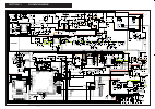
11 - 1 section 11 voltage diagram *; refer to “parts list.” 220k r175 r295 47k 330k r517 c42 0.001 r510 47k r88 560 d2 8 rb706f r243 4.7k c43 0.001 r35 100 r220 22k 4.7k r501 r185 6.8k 0.001 c171 r118 220k c226 0.001 220k r331 r69 10k ic17 njm2870 1 ctrl 2 gnd 3 nb 4 vout 5 vi n 0 r526 s1 evq-pul 1k...
Page 30
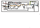
11 - 2 to the main unit to the main unit 9230b-1-02z140-pt1 j702 1 2 0.01 c716 0 r734 c742 0.001 220 r737 15p c731 11p c734 cp06s r715 470 l704 8.6n r730 2.2k r710 4.7k 0.001 c757 47p c748 q704 2sc500 6 18p c704 100p c729 q701 rd07mvs2 d703 rb706f 47p c758 imsa-6176s-03y902 j701 1 2 3 4 5 0 r736 l71...
Page 31: Section 12
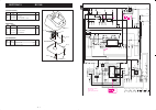
12 - 1 q1 2sc4081 r4 10 r18 r3 560 r5 0.12 r35 r31 10k r37 120k r28 r38 r29 1ss355 d2 d5 1ss355 c6 10 c11 0.01 c12 0.01 c8 0.01 c25 c26 c21 c22 0.1 0.01 c28 c23 c24 10k 0.1 0.01 0.01 c27 1k 39k 0.01 0.01 0.01 c1 0.001 0.01 c3 d4 d an202k c19 c16 r17 10k r16 560k r15 c18 56k 0.01 r14 560k r13 22k c17...
Page 32
& 0hone &ax 52, % mail :ac 0hone &ax 52, % mail 5nit 0hone &ax 52, % mail #tra 0hone &ax 52, % mail #orporate 0hone &ax 52, % mail #ustomer 0hone 'lenwood (ighway 0hone &ax 52, % mail 5nit 0hone &ax 52, % mail ! !Uckland 0hone &ax 52, % mail 2oom 9ong 0hone 52, % mail 3opot 0hone &ax % mail 0hone &a...
Page 33
1-1-32, kamiminami, hirano-ku, osaka 547-0003, japan s-14113iz-c1-q © 2004−2007 icom inc..

