- DL manuals
- Icom
- Transceiver
- IC-F33GS
- Service Manual
Icom IC-F33GS Service Manual
GUIDE FOR CD
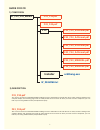
1) COMPOSION
1
IC_F33_F43_series
F33_F34.pdf
F43_F44.pdf
FYC
F33_F34_A3format.pdf
F33_F34_A4format.pdf
F43_F44_A3format.pdf
F43_F44_A4format.pdf
F33_F43_MANUAL.pdf
F34_F44_MANUAL.pdf
Installer
ar505eng.exe
W_README.txt
2) DESCRIPTION
F33_F34.pdf
The service manual for IC-F33/F34/GT/GS including all service information in this CD. This file is mainly used for viewing on the
computer display and checking page order to make printed service manual. Or when you want to find a component, you can
find very fast using “FIND” function (except Board Layout).
F43_F44.pdf
The service manual for IC-F43/F44/GT/GS including all service information in this CD. This file is mainly used for viewing on the
computer display and checking page order to make printed service manual. Or when you want to find a component, you can
find very fast using “FIND” function (except Board Layout).
Summary of IC-F33GS
Page 1
Guide for cd 1) composion 1 ic_f33_f43_series f33_f34.Pdf f43_f44.Pdf fyc f33_f34_a3format.Pdf f33_f34_a4format.Pdf f43_f44_a3format.Pdf f43_f44_a4format.Pdf f33_f43_manual.Pdf f34_f44_manual.Pdf installer ar505eng.Exe w_readme.Txt 2) description f33_f34.Pdf the service manual for ic-f33/f34/gt/gs i...
Page 2
2 f33_f34_a4format.Pdf f43_f44_a4format.Pdf consists of a4 format pages (circuit description, adjustment procedures, parts list, and etc.). This file is used for printing out a4 format pages. F33_f43_manual.Pdf the instruction manual for ic-f33/f43/gt/gs. The contents of this file is exactly same as...
Page 3: Service
Vhf transceivers service manual cover.Indd 1 10/27/2004 10:04:41 am.
Page 4
Introduction danger ordering parts this ser vice manual describes the latest ser vice information for the ic-f33gt/gs and ic-f34gt/gs vhf transceiversat the time of publication. Never connect the transceiver to an ac outlet or to a dc power supply that uses more than 8 v. Such a connection could cau...
Page 5
Table of contents section 1 specifications section 2 inside views section 3 disassembly instructions section 4 circuit descripiton 4-1 receiver circuits. . . . . . . . . . . . . . . . . . . . . . . . . . . . . . . . . . . . . . . . . . . . . . . . . . . . . . . . 4-1 4-2 transmitter circuits . . . ....
Page 6: Section 1 Specifications
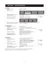
■ general • frequency coverage : 136.000–174.000 mhz • mode : fm • type of emission : • number of conventional channels : 256 ch, 16 banks • antenna impedance : 50 Ω (nominal) • operating temperature range : –30˚c to +60˚c (–22˚f to +140˚f) [usa], [gen] –25˚c to +55˚c [eur] • power supply requiremen...
Page 7: Section
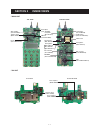
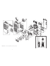
Section 2 inside views • main unit 2 - 1 • pa unit tx mute switch (q501: unr9213j) pll ic (ic21: lmx2352tm) base band ic (ic14: ak2346) eeprom (ic10: 24lc64t-i/sn) cpu (ic22: hd64f2238btf13) r5 regulator (q25: 2sa1577) fm if ic (ic9: ta31136fn) af amplifier (ic15: ta7368f) apc amplifier (ic2: ta75s0...
Page 8: Section 3
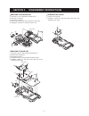
Section 3 disassembly instructions 3 - 1 chassis unit e a b c d f main shield main unit k k j j l j i g h chassis unit m n n • removing the chassis unit 1 unscrew 1 nut a, and remove 2 knobs b, c. 2 unscrew 2 screws d. 3 unscrew 2 screws e. 4 take off the chassis unit in the direction of the arrow. ...
Page 9: Section 4
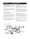
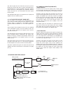
4 - 1 4-1 receiver circuits 4-1-1 antenna switching circuit (pa unit) the antenna switching circuit functions as a low-pass filter while receiving and a resonator circuit while transmitting. This circuit does not allow transmit signals to enter the receiver circuits. Received signals enter the anten...
Page 10
4 - 2 the 2nd if signal from the 2nd mixer (ic9, pin 3) passes through the ceramic filter (fi2) to remove unwanted hetero- dyned frequencies. It is then amplified at the limiter amplifier section (ic9, pin 5) and applied to the quadrature detector section (ic9, pins 10, 11) to demodulate the 2nd if ...
Page 11
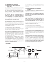
4 - 3 4-2 transmitter circuits 4-2-1 microphone amplifier circuit (main unit) the microphone amplifier circuit amplifies audio signals within +6 db/octave pre-emphasis characteristics from the microphone to a level needed for the modulation circuit. This transceiver employs the base band ic which is...
Page 12
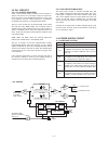
4-3 pll circuits 4-3-1 pll circuit (main unit) a pll circuit provides stable oscillation of the transmit fre- quency and receive 1st lo frequency. The pll output com- pares the phase of the divided vco frequency to the refer- ence frequency. The pll output frequency is controlled by the divided rati...
Page 13
4 - 5 4-5 other circuits 4-5-1 compander circuit (main unit) ic-f33gt/gs/f34gt/gs have compander circuit which can improve s/n ratio and become wide dynamic range. The cir- cuit is composed in the base band ic (ic14). (1) in case of transmitting the audio signals from the microphone are applied to t...
Page 14
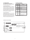
4 - 6 pin number port name description 13, 15, 16 cenc0– cenc2 output the ctcss/dtcs signals. 29 ref outputs the reference oscillator cor- recting voltage. The voltage is applied to the buffer amplifi er (ic24, pin 3) 30 plst outputs strobe signals to the pll ic (ic21, pin 16). 34 pmfm o u t p u t s...
Page 15: Section 5
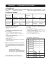
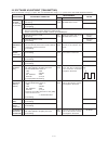
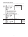
Equipment grade and range equipment grade and range dc power supply output voltage current capacity : 7.2 v dc : 5 a or more audio generator frequency range measuring range : 300–3000 hz : 1–500 mv fm deviation meter frequency range measuring range : dc–800 mhz : 0 to ±10 khz attenuator power attenu...
Page 16
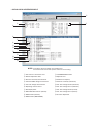
5 - 2 q: transceiver's connection state w: reload adjustment data e: receive sensitivity measurement r: connected dc voltage measurement t: pll lock voltage measurement y: operating channel select u: rf output power i: fm modulation balance (narrow) o: fm deviation (narrow) !0: fm deviation (wide/mi...
Page 17
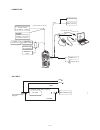
Fm deviation meter sinad meter speaker (8 Ω ) audio generator ac millivoltmeter to the antenna connector attenuator 20 db or 30 db rf power meter 0.1−10 w/50 Ω frequency counter standard signal generator 0.1 µv to 32 mv (−127 dbm to −17 dbm) caution! Do not transmit while an ssg is connected to the ...
Page 18
5 - 4 adjustment adjustment condition measurement value unit location pll lock voltage [lv (rx lva)] [lv (tx lva)] 1 • operating channel : ch7 • receiving pc screen check the "lvin" item on the cs-f33g adj's screen. 3.5 v 3.5 v 2 • operating channel : ch7 • transmitting convenient: the pll lock volt...
Page 19
5 - 5 adjustment adjustment condition measurement value unit location rx sensitivity [bpf t1] [bpf t2] 1 • operating channel : ch5 • connect the ssg to the antenna connector and set as: frequency : 136.000 mhz level : 10 µv* (–87 dbm) modulation : 1 khz deviation : ±3.5 khz • receiving pc screen con...
Page 20: Section 6
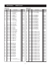
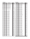
6 - 1 section 6 parts list m.=mounted side (t: mounted on the top side, b: mounted on the bottom side) [main unit] ref order description m. H/v no. No. Location [main unit] ref order description m. H/v no. No. Location ic2 1110002750 s.Ic ta75s01f (te85r) t 88.1/12.4 ic6 1110005340 s.Ic njm12902v-te...
Page 21
S.=surface mount 6 - 2 m.=mounted side (t: mounted on the top side, b: mounted on the bottom side) [main unit] ref order description m. H/v no. No. Location [main unit] ref order description m. H/v no. No. Location r82 7030009320 s.Res erj2gej 4r7 x (4.7 Ω) b 74.8/25.7 r83 7030008340 s.Res rr0510p-1...
Page 22
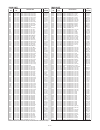
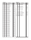
S.=surface mount 6 - 3 m.=mounted side (t: mounted on the top side, b: mounted on the bottom side) [main unit] ref order description m. H/v no. No. Location [main unit] ref order description m. H/v no. No. Location r511 7030005210 s.Res erj2gej 822 x (8.2 k Ω) b 36.5/17.8 r512 7030005210 s.Res erj2g...
Page 23
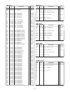
S.=surface mount 6 - 4 m.=mounted side (t: mounted on the top side, b: mounted on the bottom side) [main unit] ref order description m. H/v no. No. Location [main unit] ref order description m. H/v no. No. Location c240 4030017460 s.Cer ecj0eb1e102k b 56.8/29.8 c241 4030017460 s.Cer ecj0eb1e102k b 6...
Page 24
S.=surface mount 6 - 5 m.=mounted side (t: mounted on the top side, b: mounted on the bottom side) [pa unit] ref order description m. H/v no. No. Location [pa unit] ref order description m. H/v no. No. Location q701 1560001230 s.Fet rd07mvs1 b 22.6/8.3 q702 1560001240 s.Fet rd01mus1 b 16/8.3 q704 15...
Page 25: Section 7
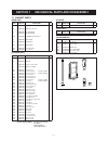
Section 7 mechanical parts and disassembly 7 - 1 7-1 cabinet parts [main unit] [chassis unit] [pa unit] ref. Order. No. Description qty. Sp1 2510001060 k036na500-47 1 w1 8900009640 opc-963 1 j1 6910015910 antenna connector-104 1 j2 6910015860 imsa-6277s-02a-g 1 mp1 8010019451 2721 chassis-1 1 mp2 82...
Page 26
7 - 2 mp2(c) mp25(c) mp30(c) mp29(c) mp33(c) mp20(c) sp1(c) mp12(c) main unit mp28(c) mp37(c) mp42(c) mp4(m) ep7(m) ds3(m) mp3(m) mp21(c) mp22(c) mp34(c) mp28(c) s27(m) r315(m) mp28(c) pa unit fuse unit mp28(c) mp38(c) j901(f) j702(p) mp47(c) ant unit mp1(c) j1(c) mp36(c) mp35(c) mp17(c) mp8(c) mp31...
Page 27
Section 8 semiconductor information 8 - 1 • diodes • transistors and fet’s 2sa1577 q (symbol: hp) xp1214 (symbol: 9h) rd01mus1 (symbol: k2) rd07mvs1 (symbol: rd07mvs1) unr9113j (symbol: 6c) unr9213j (symbol: 8c) unr9210j (symbol: 8l) xp6501 ab (symbol: 5n) 3sk299 u73 (symbol: u73) 2sc4226 r25 (symbo...
Page 28
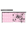
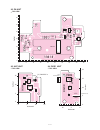
C24 r303 r13 r302 c176 s1 r130 r175 r32 c51 r31 r19 r173 r172 r23 c186 r17 c36 c43 r98 d8 q20 c42 r525 c110 c329 c328 c137 r228 r116 r40 c71 c390 ic21 c506 c508 r307 r89 l42 c139 c109 r502 r101 r44 c70 c69 r100 c141 c135 c413 c393 c375 c376 c402 c330 r229 r225 c322 r522 c368 r15 c184 c185 r22 c37 r2...
Page 29
• bottom view s5 s2 q38 l31 j3 j2 fi2 s2 mp1 q5 l13 c324 ic17 q7 x1 c75 j6 l11 l48 q15 q16 q29 l47 x2 ic6 q40 ic13 ic14 x5 d28 q44 q502 ic10 j5 1 ic22 ic12 c309 c211 ic19 ic23 c357 ic8 q27 s3 s4 d14 c45 l41 c105 r123 c142 c171 c147 c159 c515 r104 r104 r516 r154 r157 r509 r508 r301 c371 r184 c225 r18...
Page 30
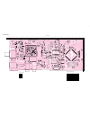
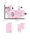
C734 r706 r705 c759 c758 mp701 l705 c719 c716 c715 c757 l704 c711 r703 c707 c708 r735 r732 c727 ep711 r730 r715 r737 c731 c763 c725 r734 q704 c728 l707 c761 c760 r733 c733 c732 c768 c706 c701 c745 c705 l709 d702 c746 c744 d705 c742 d701 l708 l703 15 20 25 30 0 5 10 v e rtical 15 20 25 30 0 5 10 35 4...
Page 31
9 - 4 • bottom view • bottom view l701 q701 c753 r726 c754 c751 j702 r701 c702 c703 c704 d703 d704 d706 l712 c750 c752 c769 c718 q702 c720 r704 r738 l702 c755 c767 c756 r736 c748 r708 c722 r729 r709 r710 c723 j701 c724 l706l706 f701 b6195b 1 3 t5v apc tx j701 to the main unit p_det gnd vcc vcc vcc t...
Page 32
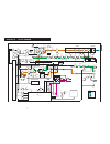
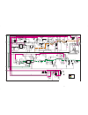
Section 10 block diagram 10 - 1 notes : contorol line common line tx line rx line data lime voltage line bpf 272.0-440.7 mhz d mute q502: 2sk3019 pre empha ic25: tc7s66fu sw lpf lpf ic6: njm12902 lpf ic19: njm12904s lpf ic6: njm12902v lpf ic6: njm12902v det pwr d701: 1sv307 d703: rb706f mute sw q501...
Page 33
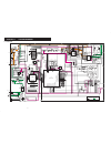
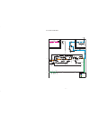
Section 11 voltage diagram 11-1 main unit r510 47 k r93 33 k r514 100 k +5v c35 0.0022 r512 8.2 k ic14 ak2346 9 10 11 12 24 23 22 21 agndin agnd txin txino limlv extlmin mod vss tclk tdata di/o rdf/fc test rxin rxino rxlpfo rxaf rxafin expout vdd xin xout dir sclk r513 47 k 24 23 22 21 20 19 18 17 1...
Page 34
11 - 2 15.3 mhz 1.2vp-p t: 0.0 r: 4.8 t: 0.0 r: 0.3 t: 0.8 r: 1.2 t: 0.0 r: 4.8 t: 0.0 r: 4.8 t: 0.0 r: 0.9 t: 1.5 r: 1.6 t: 1.6 r: 1.4 c: 3.8 c: 3.9 t: 0.0 r: 2.0 t: 0.0 r: 4.6 t: 0.0 r: 1.8 t: 0.0 r: 0.6 c: 4.0 t: 0.0 r: 4.9 t: 5.0 r: 0.0 c: 5.0 t: 2.0 r: 0.0 c: 6.9 vcc t5v s5v +5v r104 47 k c404 ...
Page 35
11-2 pa / ant / fuse units pa ant fuse l802 50 nh l801 32 nh j1(chassis) tx r801 0.001 c803 24 p l901 blm21p300s vcc gnd j901 9230b-1_02z141-t vcc 2 1 c901 0.001 vcc1 c732 0.001 c733 47 p f701 2 1 4 5 j701 imsa-6176s-03a 3 2 1 t5v tx apc vcc vcc p_det p_det gnd gnd r737 220 r730 2.2 k r715 470 r732 ...
Page 36
Asia icom inc. 6f n o.6 8 , sec. 1 cheng-teh road, taipei, tai w an, r.O.C. Phone : + 88 6 (02) 2559 1 8 99 fax : + 88 6 (02) 2559 1 8 74 url : http:// www .Asia-icom.Com e-mail : sales@asia-icom.Com zac de la plaine, 1, r u e brindejonc des mo u linais bp 5 8 04, 31505 to u lo u se cedex, france ph...
Page 37
1-1-32, kamiminami, hirano-ku, osaka, 547-0003, japan s-14113iz-c1 © 2004 icom inc. Cover.Indd 4 10/26/2004 7:26:44 pm.

