- DL manuals
- Keithley
- Multimeter
- 2000
- Repair Manual
Keithley 2000 Repair Manual
Summary of 2000
Page 1
Model 2000 multimeter repair manual a g r e a t e r m e a s u r e o f c o n f i d e n c e.
Page 2: Warranty
Warranty keithley instruments, inc. Warrants this product to be free from defects in material and workmanship for a period of 3 years from date of shipment. Keithley instruments, inc. Warrants the following items for 90 days from the date of shipment: probes, cables, rechargeable batteries, diskette...
Page 3
Model 2000 multimeter repair manual ©1995, keithley instruments, inc. All rights reserved. Cleveland, ohio, u.S.A. Second printing, march 1997 document number: 2000-902-01 rev. B.
Page 4: Manual Print History
Manual print history the print history shown below lists the printing dates of all revisions and addenda created for this manual. The revision level letter increases alphabetically as the manual undergoes sub- sequent updates. Addenda, which are released between revisions, contain important change i...
Page 5: Afety Precautions
The following safety precautions should be observed before using this product and any associated instrumentation. Although some instruments and accessories would normally be used with non-hazardous voltages, there are situations where hazardous conditions may be present. This product is intended for...
Page 6
Bles or jumpers, installing or removing switching cards, or making internal changes, such as installing or removing jumpers. Do not touch any object that could provide a current path to the common side of the circuit under test or power line (earth) ground. Al- ways make measurements with dry hands ...
Page 7: Table of Contents
Table of contents 1 routine maintenance introduction..........................................................................................1-2 setting line voltage and replacing fuse ................................................1-2 amps fuse replacement ...........................................
Page 8: List of Illustrations
List of illustrations 1 routine maintenance power module...................................................................................... 1-3 2 troubleshooting power supply block diagram ............................................................... 2-6 digital circuitry block diagram ...........
Page 9: List of Tables
List of tables 1 routine maintenance fuse rating ...........................................................................................1-3 2 troubleshooting power supply circuits...........................................................................2-7 display board checks ....................
Page 10
1 routine maintenance.
Page 11: Introduction
Introduction the information in this section deals with routine type maintenance that can be performed by the operator. This information is arranged as follows: • setting line voltage and replacing fuse — explains how to select the alternate power line voltage setting, and how to replace a blown pow...
Page 12
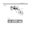
Table 1-1 fuse rating line voltage fuse rating keithley part no. 100/120v 220/240v 0.25a slow-blow 5 × 20mm 0.125a slow-blow 5 × 20mm fu-96-4 fu-91 figure 1-2 power module model 2000 warning: no internal operator servicable parts,service by qualified personnel only. Warning: no internal operator ser...
Page 13: Amps Fuse Replacement
Amps fuse replacement warning make sure the instrument is disconnected from the power line and other equipment before replacing the amps fuse. 1. Turn off the power and disconnect the power line and test leads. 2. From the front panel, gently push in the amps jack with your thumb and rotate the fuse...
Page 14
2 troubleshooting.
Page 15: Introduction
Introduction warning the information in this section is intended for qualified service personnel. Some of these procedures may expose you to hazardous voltages. Do not per- form these hazardous procedures unless you are qualified to do so. This section of the manual will assist you in troubleshootin...
Page 16: Repair Considerations
Repair considerations before making any repairs to the model 2000, be sure to read the following considerations. Caution the pc-boards are built using surface mount techniques and require special- ized equipment and skills for repair. If you are not equipped and/or qualified, it is strongly recommen...
Page 17: Front Panel Tests
Front panel tests there are two front panel tests: one to test the functionality of the front panel keys and one to test the display. In the event of a test failure, refer to “display board checks” for details on trou- bleshooting the display board. Key test the key test allows you to check the func...
Page 18: Principles of Operation
Principles of operation the following information is provided to support the troubleshooting tests and procedures covered in this section of the manual. Refer to the following block diagrams: block diagrams: figure 2-1 — power supply block diagram figure 2-2 — digital circuitry block diagram figure ...
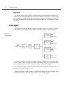
Page 19: Power Supply
Key matrix the front panel keys (s401-s430) are organized into a row-column matrix to minimize the number of microcontroller peripheral lines required to read the keyboard. A key is read by strob- ing the columns and reading all rows for each strobed column. Key down data is interpreted by the displ...
Page 20: Digital Circuitry
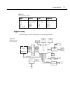
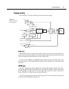
Digital circuitry refer to figure 2-2 for the following discussion on digital circuitry. Table 2-1 power supply circuits supply rectifier filter regulator +5vd +37v +15v -15v +5v, +5vrl cr104 cr116, cr117 cr102 cr102 cr103 c128, c156 c104, c108 c148 c131 c146 u144 u101 u125 u119 u124 figure 2-2 digi...
Page 21
Microprocessor u135 is a 68306 microprocessor that oversees all operating aspects of the instrument. The mpu has a 16-bit data bus and provides an 18-bit address bus. It also has parallel and serial ports for controlling various circuits. For example, the rxda, txda, rxdb and txdb lines are used for...
Page 22: Analog Circuitry
Analog circuitry refer to figure 2-3 for the following discussion on analog circuitry. Input hi input hi protection is provided by the ssp (solid state protection) circuit. The ssp is pri- marily made up of q101 and q102. An overload condition opens q101 and q102. This discon- nects the analog input...
Page 23
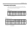
Signal switching signal switching for dcv and ohms is done by the dcv & ohms switching circuit. Fets q113, q105, q104 and q108 connect the dcv or ohms signal to the × 1 buffer (u113). (tables 2-5 through 2-8 show the switching states of these fets for the various dcv and ohms ranges.) note that the ...
Page 24: Display Board Checks
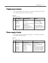
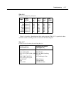
Display board checks if the front panel disp test indicates that there is a problem on the display board, use table 2-2. See “principles of operation” for display circuit theory. Power supply checks power supply problems can be checked out using table 2-3. See “principles of operation” for circuit t...
Page 25: Digital Circuitry Checks
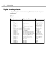
Digital circuitry checks digital circuit problems can be checked out using table 2-4. See “principles of operation” for digital circuit. Table 2-4 digital circuitry checks step item/component required condition remarks 1 2 3 4 5 6 7 8 9 10 11 12 13 14 15 16 17 power-on test u152 pin 16 u152 pin 32 u...
Page 26
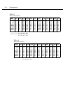
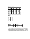
Analog signal switching states tables 2-5 through 2-11 provide switching states of the various relays, fets and analog switches for the basic measurement functions and ranges. These tables can be used to assist in tracing an analog signal from the input to the a/d multiplexer. Table 2-5 dcv signal s...
Page 27
Table 2-7 Ω 2 signal switching range q101 q102 q114 q136 q109 k101* k102* q113 q105 q104 q108 q121 100 Ω 1k Ω 10k Ω 100k Ω 1m Ω 10m Ω 100m Ω on on on on on on on on on on on on on on off off off off off off off off off off off off off off off off off off off on on set set set set set set set reset r...
Page 28
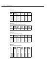
Tables 2-12 through 2-16 can be used to trace the analog signal through the a/d multiplexer (u163) to the final amplifier stage. These tables show the mux lines (s3, s4, s6, s7) that are selected for measurement during the signal phase of the multiplexing cycle. Also included are switching states of...
Page 29
Table 2-12 dcv signal multiplexing and gain range signal (u163) u129 pin 1 u129 pin 8 u129 pin 9 gain (u166) 100mv 1v 10v 100v 1000v s4 s4 s4 s4 s4 off off on off on off on off on off on off off off off × 100 × 10 × 1 × 10 × 1 table 2-13 acv and aca signal multiplexing and gain range signal (u163) u...
Page 30
Figure 2-3 provides a block diagram of the analog circuitry. Table 2-17 is provided to show where the various switching devices are located in the block diagram. Table 2-16 Ω 4 signal multiplexing and gain range signal (u163) u129 pin 1 u129 pin 8 u129 pin 9 gain (u166) 100 Ω 1k Ω 10k Ω 100k Ω 1m Ω ...
Page 31: Built-In Test Overview
Built-in test overview built-in test is used to test and exercise various circuits and components. The built-in tests are listed in table 2-18. Many of the tests are actual pass/fail type tests, while others are circuit exercises that are used for subsequent tests. Each built-in test can be run manu...
Page 32
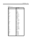
Table 2-18 built-in test summary test circuit tested bank 100 100.1 100.2 101.1 101.2 101.3 bank 200 200.1 200.2 201.1 201.2 bank 300 300.1 301.1 301.2 302.1 302.2 303.1 303.2 304.1 bank 400 400.1 400.2 400.3 401.1 401.2 401.3 402.1 402.2 402.3 403.1 403.2 403.3 bank 500 500.1 500.2 bank 600 600.1 6...
Page 33: Auto Testing
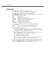
Auto testing 1. Press shift and then test to access the self-test options. 2. Use the ▲ or ▼ key to display “test: built-in” and press enter. 3. Use the ▲ or ▼ key to display “bit: auto” and press enter. 4. Use the , , ▲ or ▼ key to display the bank of tests that you wish to run and press enter. Tes...
Page 34: Manual Testing
Manual testing 1. Press shift and then test to access the self-test options. 2. Use the ▲ or ▼ key to display “test: built-in” and press enter. 3. Use the ▲ or ▼ key to display “bit: manual” and press enter. 4. Use the and keys, or the ▲ and ▼ keys to display the desired test series number. For exam...
Page 35: Built-In Test Documentation
Built-in test documentation the following paragraphs provide a detailed description of each built-in test. Refer to “built-in test overview” for basic information on how to use built-in tests. The following doc- umentation is provided for each test: • test identification — includes test bank, number...
Page 36: Test Bank: A/d
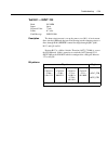
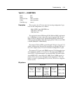
Test bank: a/d test 100.1 — a/d bank a/d inputs open expected value 153661550 counts limits 1200000 counts fault message no a/d comm description this a/d test uses the default conditions of the adc word and the acdc word. This sets up the front end of the instrument to a stable configuration. The mu...
Page 37
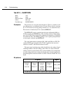
Test 100.2 — a/d bank a/d inputs open expected value limits 100 counts fault message signal noisy description this test has the identical setup as the 100.1 test. Signal lo is connected to the a/d circuit for ten readings and a min/max comparison is done to en- sure that all readings are within 100 ...
Page 38
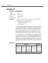
Test 101.1 — testcal bank a/d expected value limits inputs open description testcal is a way to calibrate the unit with internal references so that the remaining tests can be displayed in the form of voltages. Given that there are errors in the internal references and in the a/d circuitry, the volta...
Page 39
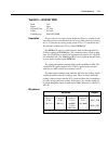
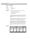
Test 101.2 — testcal bank a/d inputs open expected value (101.2) - (101.1) = 76275970 counts limits 1800000 fault message no 7v at a/d description this a/d test uses the default conditions of the adc word and the acdc word. This sets up the front end of the instrument to a stable configuration. The ...
Page 40
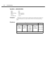
Test 101.3 — testcal bank a/d inputs open expected value 1.03 volts limits 0.06 volts fault message no 1v at a/d description this test uses the default conditions of the adc word and the acdc word. This sets up the front end of the instrument to a stable configuration. The mux word sets shift regist...
Page 41: Test Bank: Ref/mux
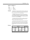
Test bank: ref/mux test 200.1 — reference bank ref/mux inputs open expected value 1 volt limits 0.1 volts fault message 1vref/ad x10 description the 7v refhi signal is routed through r189 and r185, which forms a 0.014/1 voltage divider with r188. The 0.1v result (0.014 × 7v = 0.1v) is then applied t...
Page 42
Test 200.2 — reference bank ref/mux inputs open expected value 10 volts limits 1 volt fault message ad x100 description same as test 200.1 except the a/d mux is configured for × 100 gain (/ × 100 control line is low). The gain path is through u129 pin 10 to 11. Resis- tor network r271 is used to con...
Page 43
Test 201.1 — a/d mux lo bank ref/mux inputs open expected value 0 volts limits 0.0001 volts fault message sense lo 0 description signal lo is routed through r181 and q122 (/lomuxa control line high) into unity gain amp u126. Signal lo is then routed to s7 of u163. The a0, a1 and a2 bit pattern on u1...
Page 44
Test 201.2 — a/d mux lo bank ref/mux inputs open expected value 0 volts limits 0.0001 volts fault message mux lo description this test is similar to test 201.1, except signal lo is routed through r274 to s8 of u163. Signal lo is then routed through q117 to u166, which is con- figured for × 1 gain. M...
Page 45: Test Bank: Dc/ohm
Test bank: dc/ohm test 300.1 — front end lo bank dc/ohm inputs open expected value 0 volts limits 0.01 volts fault message front end lo description this test is for the dc volts front end lo path. Control line divlo is high making the u120 comparator output (pin 2) open collector. Q114 is on due to ...
Page 46
Test 301.1 — hi ohms bank dc/ohm inputs open expected value 7 volts limits 0.7 volts fault message 7v refboot description +7v is generated by buffering refhi with op amp u139. This +7v, which is used by the ohms circuit as a voltage reference, is switched by u133 (/7v control line low) to op amp u12...
Page 47
Test 301.2 — hi ohms bank dc/ohm inputs open expected value 12.4 volts limits 0.5 volts fault message 13.3 refboot description this test is the same as 301.1 except that the +13.3v ohms reference is tested. The +13.3v reference is generated by the same circuit as the +7v ref- erence. 14v is routed t...
Page 48
Test 302.1 — 2w sense bank dc/ohm inputs open expected value 7 volts limits 0.7 volts fault message 2w sense 7v description the +7v reference is again switched to refboot, and routed through r272, q109, the 9.9m Ω half of divider r117, the parallel combination of r115, r324 and l109, and then throug...
Page 49
Test 302.2 — 2w sense bank dc/ohm inputs open expected value 12.4 volts limits 0.5 volts fault message 2w sense 13v description same as test 302.1 except the +13.3v reference is used. This voltage does not go through the ohms zener clamp path but is clipped by the a/d circuit itself at about 12.4v d...
Page 50
Test 303.1 — lo ohm path bank dc/ohm inputs open expected value 7 volts limits 0.7 volts fault message 7v source description this test uses the ohms circuit. The +7v reference is switched to ref- boot by closing u133 (/7v line low). Q123 and q125 are turned on by set- ting the ohma control line high...
Page 51
Test 303.2 — lo ohm path bank dc/ohm inputs open expected value 12.4 volts limits 0.5 volts fault message 13.3v source description this test is similar to test 303.1. The +13.3v reference is switched to ref- boot again by closing u133 pins 6 to 7. Q124 and q126 are turned on by setting the ohma cont...
Page 52
Test 304.1 — input /100 bank dc/ohm inputs open expected value 7 volts limits 0.7 volts fault message inp sig/100 description the ohms circuit current is set up the same as test 303.1. A 1ma current flows into the ohm node but instead of flowing into the clamping circuit, it flows through k101 (rese...
Page 53: Test Bank: Vac
Test bank: vac test 400.1 — non inv path bank vac inputs open expected value limits fault message description this test places the acv front end in the non-inverting configuration. Logic levels for this configuration are as follows: k102: /setk1 low, /resetk1 high u103: pins 8 and 9 low u105: pin 9 ...
Page 54
Test 400.2 — non inv path bank vac inputs open expected value 5.6 volts limits 0.6 volts fault message non inv path description the previous test sets up the circuit for this test. There is a routine in soft- ware that generates a waveform for the acv tests. This is done by selecting the 13.3v refer...
Page 55
Test 400.3 — non inv path bank vac inputs open expected value limits fault message description this phase resets the circuit to a known state and turns the waveform sig- nal off. Subsequent tests require that the a/d be in the normal operating mode. Bit patterns bit pattern register q q 87654321 —u1...
Page 56
Test 401.1 — invert path bank vac inputs open expected value limits fault message description this test places the acv front end in the inverting configuration. Logic levels for this configuration are as follows: k102: /setk1 high, /resetk1 low u103: pins 8 and 9 high u105: pin 9 low the signal path...
Page 57
Test 401.2 — invert path bank vac inputs open expected value 0.108 volts limits 0.02 volts fault message invert path description the previous test sets up the circuit for this test. There is a routine in soft- ware that generates a waveform for the acv tests. This is done by selecting the 13.3v refe...
Page 58
Test 401.3 — invert path bank vac inputs open expected value limits fault message description this phase resets the circuit to a known state and turns the waveform sig- nal off. Subsequent tests require that the a/d be in the normal operating mode. Bit patterns bit pattern register q q 87654321 —u10...
Page 59
Test 402.1 — non inv /10 bank vac inputs open expected value limits fault message description this test places the acv front end in the non-inverting configuration. Logic levels for this configuration are as follows: k102: /setk1 low, /resetk1 high u103: pins 8 and 9 low u105: pin 9 high the signal ...
Page 60
Test 402.2 — non inv /10 bank vac inputs open expected value 0.108 volts limits 0.02 volts fault message non inv /10 description the previous test sets up the circuit for this test. There is a routine in soft- ware that generates a waveform for the acv tests. This is done by selecting the 13.3v refe...
Page 61
Test 402.3 — non inv /10 bank vac inputs open expected value limits fault message description this phase resets the circuit to a known state and turns the waveform sig- nal off. Subsequent tests require that the a/d be in the normal operating mode. Bit patterns bit pattern register q q 87654321 —u10...
Page 62
Test 403.1 — non inv bex2 bank vac inputs open expected value limits fault message description this test places the acv front end in the non-inverting configuration. Logic levels for this configuration are as follows: k102: /setk1 low, /resetk1 high u103: pins 8 and 9 low u105: pin 9 high the signal...
Page 63
Test 403.2 — non inv bex2 bank vac inputs open expected value 1.08 volts limits? 0.2 volts fault message non inv bex2 description the previous test sets up the circuit for this test. There is a routine in soft- ware that generates a waveform for the acv tests. This is done by selecting the 13.3v ref...
Page 64
Test 403.3 — non inv bex2 bank vac inputs open expected value limits fault message description this phase resets the circuit to a known state and turns the waveform sig- nal off. Subsequent tests require that the a/d be in the normal operating mode. Bit patterns bit pattern register q q 87654321 —u1...
Page 65: Test Bank: Sense
Test bank: sense test 500.1 — 4w sense bank sense inputs 4-wire short expected value 0 volts limits 0.0001 volts fault message sense lo description this test requires a 4-wire short at the input. The slo node is the sense lo jack on the front or rear panel. The 4-wire short connects slo to lo. The 0...
Page 66
Test 500.2 — 4w sense bank sense inputs 4-wire short expected value 0 volts limits 0.0001 volts fault message sense hi description this test requires a 4-wire short at the input. The shi node is the sense hi jack on the front or rear panel. The 4-wire short connects shi to lo. The 0v signal at shi i...
Page 67: Test Bank: Amp/ohm
Test bank: amp/ohm test 600.1 — ohm/amp bank amp/ohm inputs input hi to amps short expected value 0.0095 volts limits 0.001 volts fault message 1ma source description this test requires a jumper wire from the input hi jack to the amps jack on the front panel. The +7v reference is switched to the ohm...
Page 68
Test 600.2 — ohm/amp bank amp/ohm inputs input hi to amps short expected value 0.025 volts limits 0.015 volts fault message .1 ohm shunt description this test requires a jumper wire from the input hi jack to the amps jack on the front panel. The +7v reference is switched to the ohms circuit through ...
Page 69
Test 601.1 — amp shunt bank amp/ohm inputs input hi to amps short expected value limits fault message description this test requires an external jumper wire be installed from the input hi jack to the amps jack on the front panel. There is a routine in software that generates a test signal current fo...
Page 70
Bit patterns bit pattern register q q 87654321 —u106— 110v0010 q q 87654321 —u109— 11011111 q q 87654321 —u134— 1v10110v —u130— 10011101 q q 87654321 —u121— 10110000 acdc_stb mux_stb ic pins: q8=11, q7=12, q6=13, q5=14, q4=7, q3=6, q2=5, q1=4 troubleshooting 2-57.
Page 71
Test 601.2 — amp shunt bank amp/ohm inputs input hi to amps short expected value 0.084 volts limits 0.02 volts fault message ac amp shunt description the previous test sets up the circuit for this test. There is a routine in soft- ware that generates a waveform for the acv tests. This is done by sel...
Page 72
Test 601.3 — amp shunt bank amp/ohm inputs input hi to amps short expected value limits fault message description this phase resets the circuit to a known state and turns the waveform sig- nal off. Subsequent tests require that the a/d be in the normal operating mode. Bit patterns bit pattern regist...
Page 73
3 disassembly.
Page 74: Introduction
Introduction this section explains how to handle, clean, and disassemble the model 2000 multimeter. This section is organized as follows: • handling and cleaning — describes how to properly handle, clean, and solder pc boards. • static sensitive devices — explains how to handle ics and cmos devices....
Page 75: Handling and Cleaning
Handling and cleaning to avoid contaminating pc board traces with body oil or other foreign matter, avoid touching the pc board traces while you are repairing the instrument. Motherboard areas covered by the shield have high impedance devices or sensitive circuitry where contamination could cause de...
Page 76: Static Sensitive Devices
Static sensitive devices cmos devices operate at very high impedance levels for low power levels. Therefore, any static that builds up on you or your clothing may be sufficient to destroy these devices if they are not handled properly. Use the following precautions to avoid damaging them: caution ma...
Page 77: Case Cover Removal
Case cover removal if you need to troubleshoot the instrument or replace a component, you must gain access to the components by removing the case. Warning before removing the case cover, disconnect the line cord and any test leads from the instru- ment. 1. Remove handle — the handle serves as an adj...
Page 78: Changing Trigger Link Lines
Changing trigger link lines the model 2000 uses two lines of the trigger link rear panel connector as external trigger (ext trig) input and voltmeter complete (vmc) output. At the factory, line 1 is configured as vmc and line 2 as ext trig. Note line 1, 3 or 5 of the trigger link can be configured a...
Page 79: Motherboard Removal
Motherboard removal perform the following steps to remove the motherboard. This procedure assumes that the case cover is already removed. 1. Remove the ieee-488 and rs-232 fasteners. The ieee-488 and the rs-232 connectors each have two nuts that secure the connectors to the rear panel. Remove these ...
Page 80: Front Panel Disassembly
Front panel disassembly use the following procedures to remove the display board and/or the pushbutton switch pad: note you must first remove the case cover, the front/rear input switch, and the front input terminal wires as described in earlier in this section. 1. Unplug the display board ribbon ca...
Page 81
Main cpu firmware replacement changing the firmware may be necessary as upgrades become available. The firmware revi- sion level for the main cpu is displayed during the power-on sequence. The firmware for the main cpu is located in the eproms u156 (even) and u157 (odd), leadless ics that resides in...
Page 82: Removing Power Components
Removing power components the following procedures to remove the power transformer and/or power module require that the case cover and motherboard be removed, as previously explained. Power transformer removal perform the following steps to remove the power transformer: 1. Remove motherboard. 2. Unp...
Page 83: Power Module Removal
Power module removal perform the following steps to remove the power module: 1. Remove motherboard. 2. Unplug the transformer wires that attach to the power module at the rear panel. During re-assembly, use drawing 2000-050 as a reference and replace the wires as fol- lows: 3. Disconnect the power m...
Page 84: Instrument Re-Assembly
Instrument re-assembly re-assemble the instrument by reversing the previous disassembly procedures. Make sure that all parts are properly seated and secured and that all connections are properly made. To en- sure proper operation, replace and securely fasten the shield. Warning to ensure continued p...
Page 89
4 replaceable parts.
Page 90: Introduction
Introduction this section contains replacement parts information and component layout drawings for the model 2000. Parts list the electrical parts lists for the model 2000 are shown in tables 4-1 to 4-3. For part numbers to the various mechanical parts and assemblies, use the miscellaneous parts lis...
Page 91: Factory Service
Factory service if the instrument is to be returned to keithley instruments for repair, perform the following: 1. Call the repair department at 1-800-552-1115 for a return material authorization (rma) number. 2. Complete the service form at the back of this manual, and include it with the instrument...
Page 92
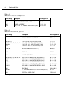
Table 4-1 model 2000 connector board, parts list circuit desig. Description keithley part no. C101 j1034 p1017 r196 cap, .1uf, 10%, 25v, ceramic (0805) conn, male rt angle, 32-pin cable assembly res, 2.21k, 1%, 100mw, thick film (0805) c-495-.1 cs-456 ca-123-14a r-418-2.21k table 4-2 model 2000 disp...
Page 93
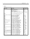
Table 4-3 model 2000 motherboard, parts list circuit desig. Description keithley part no. At101 c101,160,163,174,180,186,207 c102 c104 c105 c106 c107 c109 c112,248 c113,114,119,126,246,247 c115 c117,147,151,191,234,237 c120 c121,132,134,140 c123,245 c131,148 c135,203,198,183,187,197,249 c137 c145 c1...
Page 94
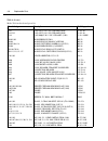
C241 c242,243 c244 cr102,103 cr104 cr105,108,114 cr106 cr110,cr118 cr111,112,115-117 e101,102 j1006 j1007 j1008 j1014 j1015 j1016 j1017 k102,101 k103 l101,103,102,104 l105,l106 l107,108 l109 ls101 q101,102 q103,110,112,115,118,128,130 q104-109,113,114,117,120-126 q119 q116,111,129 q127,131,132,133 r...
Page 95
R109 r110,133 r114 r115 r117 r122,134,272,181 r123 r127 r129 r135 r139,148,163 r142 r145,156,321,322 r146 r147 r149,151 r150 r152,143,137 r153 r154,230 r155 r157 r158 r159,166,185,275,307,314 r164,112 r168 r169,214,218 r172,167,160 r176,179,183,186,193,130,177 r178,184,187,161,213,257,248 r188 r189 ...
Page 96
R220,221,264,212,217 r225 r226,228,235,237,250,252,255 r234 r238,244,254,293 r241 r243,259 r245 r246 r261 r267,270 r271 r273,274 r277 r279,140,256,299 r280,294 r283 r287 r288,289,290 r291,292 r295,118,175,276,282,316 r297,278,281 r300 r302,303 r304 r309 r310 r311 r312,313 r315 r317,320 r318 r324 s10...
Page 97
U106,109,121,130,134 u107,108 u110 u112 u113 u114 u116 u117,145 u119 u120,131,115 u123 u124 u125 u126 u133 u135 u136 u137,166 u138,132 u139 u141 u142 u144 u146 u147,164 u148,153 u149 u150 u151,152 u154 u155 u156 u157 u158 u159 u160 u161 u162 u163 ic, 8 stage shift/store,mc14094bd(soic) ic, photo, da...
Page 98
Vr101,114 vr102 vr103,104 vr105,106,115,116 vr107,108 vr109 vr110 vr112,113 y101 y102 var, 576v metal oxide diode, zener 6.2v, bzx84b6v2 (sot-23) diode, zener, 6.8v,mmsz5235bt1 (sod-23) diode, zener 11v,mmsz11t1 (sod-123) diode, zener 3.3v, mmbz5226bl(sot-23) diode, zener 17v, mmbz5247bl (sot-23) di...
Page 99
Banana jack, push-in, black banana jack, push-in, red bezel, rear bracket, rear panel scanner cover plate cable clamp for display cable & tr-299 wire cable clamp tie wrap, nylon, 4" long for front/rear wires captive panel screw for bezel card guide/shield chassis assembly connector, hardware kit for...
Page 100
Table 4-5 model 2000 miscellaneous, parts list description keithley part no. Calibration manual package cover panel, scanner disk programming handle line cord quick reference guide package test leads user's manual package 2000-905-00 2001-372a 2000-dsk-81 428-329f co-7 2000-903-00 ca-22 2000-900-00 ...
Page 103
A specifications.
Page 104: Drn.
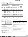
Keithley instruments, inc. Cleveland, ohio 44139 drn. Ckd. App. Date date date part number ltr revisions app. Date form 28777a-sbg bruning 40-21 62198-sbg purchased item specifications 2000 6 1 ⁄ 2 -digit multimeter dc characteristics conditions: med (1 plc) 1 or slow (10 plc) accuracy: ±(ppm of rea...
Page 105: Drn.
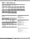
Keithley instruments, inc. Cleveland, ohio 44139 drn. Ckd. App. Date date date part number ltr revisions app. Date form 28777a-sbg bruning 40-21 62198-sbg purchased item specifications 2000 6 1 ⁄ 2 -digit multimeter true rms ac voltage and current characteristics accuracy 1 : ±(% of reading + % of r...
Page 106: Drn.
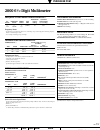
Keithley instruments, inc. Cleveland, ohio 44139 drn. Ckd. App. Date date date part number ltr revisions app. Date form 28777a-sbg bruning 40-21 62198-sbg purchased item specifications 2000 6 1 ⁄ 2 -digit multimeter frequency and period characteristics 1,2 resolution accuracy acv frequency period ga...
Page 107: Index
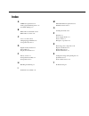
Index a amps fuse replacement 1-4 analog signal switching states 2-13 assembly drawings 3-4 b built-in test documentation 2-22 built-in test overview 2-18 c case cover removal 3-5 changing trigger link lines 3-6 components layouts 4-3 d digital circuitry checks 2-12 disassembly 3-1 display board che...
Page 108: Service Form
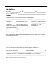
Service form model no. _________________ serial no. ______________________ date_________________ name and telephone no. ________________________________________________________ company ______________________________________________________________________ list all control settings, describe problem ...
Page 109
Specifications are subject to change without notice. All keithley trademarks and trade names are the property of keithley instruments, inc. All other trademarks and trade names are the property of their respective companies. Keithley instruments, inc. 28775 aurora road • cleveland, ohio 44139 • 440-...


