1 0 1 0 3 0 p.O.Box 1, hamamatsu, japan service manual important notice this manual has been provided for the use of authorized yamaha retailers and their service personnel. It has been assumed that basic service procedures inherent to the industry, and more specifically yamaha products, are already...
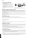
Cdc-697 cdc-697 2 wall outlet equipment under test ac leakage tester or equivalent insulating table ■ to service personnel 1. Critical components information components having special characteristics are marked z and must be replaced with parts having specifications equal to those originally install...
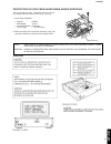
Cdc-697 3 cdc-697 this set employs a laser. Therefore, be sure to care- fully follow the instructions below when servicing. 1. Laser diode properties • material : gaalas • wavelength : 790 nm • emission duration : continuous • laser output : . 1.23 mw (max.) 2. When checking the laser diode emission...
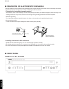
Cdc-697 cdc-697 4 ■ prevention of electrostatic discharge the laser diode in the dvd mechanism may be damaged due to static electricity from clothes or the human body. Use caution to prevent electrostatic damage when servicing or handling the dvd-mechanism. 1. Grounding for electrostatic damage prev...
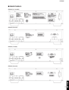
Cdc-697 5 cdc-697 ■ rear panels cdc-697 (u, c models) cdc-697 (r model) cdc-697 (t model) cdc-697 (a model).
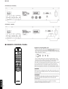
Cdc-697 cdc-697 6 cdc-697 (b, g models) cdc-697 (l model) ■ remote control panel.
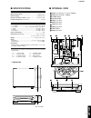
Cdc-697 7 cdc-697 ■ specifications ■ audio section output level (1 khz, 0 db) ................................................. 2 ±0.5 v signal to noise ratio .............................................. 106 db or more dynamic range .......................................................... 96 db ...
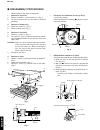
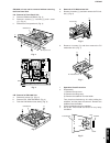
Cdc-697 cdc-697 8 ■ disassembly procedures fig. 1 (remove parts in the order as numbered.) 1. Removal of top cover a. Remove 4 screws (1) and 3 screws (2). (fig. 1) b. Lift the top cover at the rear and move it rearward slantingly. 2. Removal of clamp ass’y a. Remove 2 screws (3). (fig. 1) b. Remove...
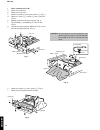
Cdc-697 9 cdc-697 cm-230a unit can not be removed without removing the front panel unit. 5-a. Removal of front panel unit a. Remove cb200 and cb304. (fig. 4) b. Remove 2 screws (7), 3 screws (8) and 1 screw (9). (fig. 3) c. Remove the front panel unit. (fig. 3) 8 9 7 7 cm-230a unit front panel unit ...
Cdc-697 cdc-697 10 • when checking the p.C.B.: a. Remove the top cover. B. Remove the tray ass’y. C. Remove 3 screws (1) and 2 jack screws (2). (fig. 1) d. Remove 1 screw (3), 1 screw (4) and 1 push rivet. (fig. 2) e. Spread a cloth over the main chassis. (fig. 2) f. Put the main (1) and main (6) p....
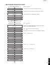
Cdc-697 11 cdc-697 ■ standard operation chart "open" is displayed. Trv signal is output until detection of feed limit switch. Press "open/close" key. Forced feed return operation. Clamp down operation. Tracking offset auto adjustment. Focus offset auto adjustment. Laser on. Disc scan. Focus gain rou...
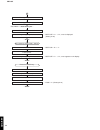
Cdc-697 cdc-697 12 press the "stop" key. Focus gain adjustment. Tracking gain adjustment. After searching the beginning, mute is cancelled. Mute on. Track search. After searching the beginning, mute is cancelled. Mute on. Spindle motor stop. Laser off. Forced feed return. *toc read * ~ data fetch cy...
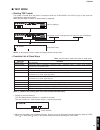
Cdc-697 13 cdc-697 ■ test mode • starting test mode test mode is started when the power is turned on while the “play/pause” and “stop” keys on the panel are simultaneously pressed and held. When the test mode is started, as shown below is displayed. Note: “traverse servo” means the same as “feed ser...
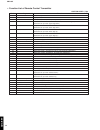
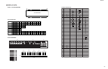
Cdc-697 cdc-697 14 mode open/close play t t t t t skip e e e e e search r r r r r search y y y y y skip repeat text/time (note 2) index prog clear 0 1 2 3 4 5 6 7 8 9 +10 random output level – output level + dimmer (note 2) disc skip w w w w w disc skip q q q q q disc scan (note 1) pause stop tape s...
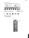
Cdc-697 15 cdc-697 (note 2) checks fl display. Dimmer text/time.
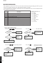
Cdc-697 cdc-697 16 error message description ■ error messages when stopped by any cause, press “stop” key of the remote control while pressing and holding the “stop” key on the main unit. The operation mode turns to the mode allowing the display of messages. The unit hold the latest error message in...
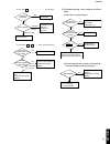
Cdc-697 17 cdc-697 2) troubleshooting from system malfunc- tions. A) tray fails to come out/go in. B) no sound generated, sound cut during play. (but time display advanced properly) error code x8 ..................................... Focus drops. Error codes x9 , xa ............ Poor clamp operation...
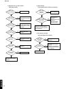
Cdc-697 cdc-697 18 c) operates as if no disc loaded. (although loaded) d) sound skips. (time display fails to advance properly) e) no search provided. (sound skipped after search) disc clamp defective. Clamp switch defective. Microprocessor (ic309) defective. Yes does disc clamp operate properly? Ic...
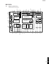
Cdc-697 19 cdc-697 ■ ic data ic3 : mn35511al (main p.C.B.) signal processor and controller 58 59 56 17 s tat x1 x2 xsel timing generator pitch control vco micro computer interface servo cpu output port d/a converter efm demodulation sync interpolation subcode demodulation circ error correction de in...
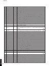
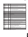
Cdc-697 cdc-697 20 1 2 3 4 5 6 7 8 9 10 11 12 13 14 15 16 17 18 19 20 21 22 23 24 25 26 27 28 29 30 31 32 33 34 35 36 37 38 39 40 41 42 43 44 45 46 47 48 49 50 pin no. Bclk lrck srdata dvdd1 dvss1 tx mclk mdata mld sense flock tlock blkck sqck subq dmute stat rst smck/ fclk clvs/ flag6 trv tvd pc ec...
Cdc-697 21 cdc-697 (note 1) at the smck/fclk pin, output does not stop while /rst=l. Pin no. Name function i/o 51 52 53 54 55 56 57 58 59 60 61 62 63 64 65 66 67 68 69 70 71 72 73 74 75 76 77 78 79 80 avss2 efm pck/ resy flag crc xsel vss x1 x2 vdd vcof2 avss1 out1c out1d out2d out2c avdd1 dempo ck3...
Cdc-697 cdc-697 22 ic309 : µpd78f0546 (main p.C.B.) microprocessor 7 8 4 2 p00 to p06 port 0 8 p10 to p17 port 1 8 p20 to p27 port 2 4 p30 to p33 port 3 8 p40 to p47 port 4 8 p50 to p57 port 5 8 p60 to p67 port 6 8 p70 to p77 port 7 5 p120 to p124 port 12 p130 port 13 6 8 p140 to p145 port 14 buz/p1...
Cdc-697 23 cdc-697 1 2 3 4 5 6 7 8 9 10 11 12 13 14 15 16 17 18 19 20 21 22 23 24 25 26 27 28 29 30 31 32 33 34 35 36 37 38 39 40 41 42 43 44 45 46 47 48 49 50 51 52 53 54 55 56 57 58 59 60 p120/intp0/exlvi p47 p46 p45 p44 p43 p42 p41 p40 /reset p124/xt2/exclks p123/xt1 flmd0 p122/x2/exclk/ocd0b p12...
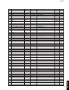
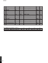
Cdc-697 cdc-697 24 pin pin function function signal name detail of function port type i/o 61 62 63 64 65 66 67 68 69 70 71 72 73 74 75 76 77 78 79 80 ani7/p27 ani6/p26 ani5/p25 ani4/p24 ani3/p23 ani2/p22 ani1/p21 ani0/p20 p130 p04//sck11 p03/si11 p02/so11 p01/ti010/to00 p00/ti000 p145/stb0 p144/soa0...
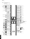
25 cdc-697 ■ display data 3g 15g 14g 13g 12g 11g s1 b1 b2 10g 9g 8g 7g 6g 5g 4g 2g 1g note : 1) f1, f2 ..... Filament pin 2) np ..... No pin 3) nx ..... No extend pin 4) ic ..... Internal connection 5) 1g-15g ..... Grid pin no. 76 f1 75 f1 74 np 73 np 72 ic 71 p1 70 p2 69 p3 68 p4 67 p5 66 p6 65 p7 ...
Cdc-697 26 ■ pin connection diagrams common output input out com in 1 4 8 1: in 2: gnd 3: out 1 8 16 36 18 1 1 3 4 5 1 16 17 32 33 48 49 64 1 10 1 4 8 40 60 61 1 41 20 21 80 kia79s05p-at njm2068d-d mn35511al njm78m05fa adm202jrn-reel7 an8882sb an4801sb bd4243g-tr m66003-0131fp lb6510 br24l01af-we2 µ...
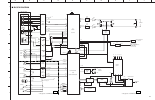
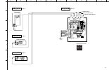
A b c d e f g h i j 1 2 3 4 5 6 7 cdc-697 27 audio section block diagram ■ block diagram ic3 ic4 9-12 78,13,14 mn35511 spc+dac head amp ic1 an8882sb m m m m m control system control ic309 8bit microprocessor ic402 ta7291p ic401 la6510-e c o n t r o l power supply sw303,307-309,312-314,317, 318,322,3...
2 a b c d e f g h i j 1 3 4 5 7 cdc-697 6 28 flsw d4gnd v o3+ v o3- v o4+ v o4- v o1+ v o2+ pd ld e c a vcca3+5 /pdn d4gnd -vb -vb1 fl1 fl2 v o2- v o1- a3gnd a3gnd b d f a3gnd vcc+b d4gnd nc tbl_r cl_up open clsw upsw mgnd -vb vccd5+5 tbl_l cl_down close opsw downsw tbl_pos fl2 flgnd cl /blk rem vcc...
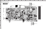
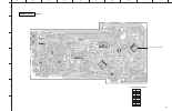
A b c d e f g h i j 1 2 3 4 5 6 7 cdc-697 29 1 1 3 4 5 1 1 1 16 17 32 33 48 49 64 4 8 5 13 14 26 80 20 21 40 41 60 61 1 8 9 16 18 36 19 no replacement part available. Main (1) p.C.B. (side b) • semiconductor location ic1 e4 ic2 e3 ic3 f5 ic4 b3 ic302 g4 ic306 g5 ic309 h3 q208 c4 q209 d4 q210 b4 ref ...
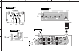
2 a b c d e f g h i j 1 3 4 5 7 cdc-697 6 30 8 5 8 5 1 1 4 4 main (1) main (4) (cb05) main (8) (w200a)(w200b) vccd+5 psw key0 flgnd main (1) disc5 disc4 disc3 disc2 disc1 standby/on main (8) (w207a) main (8) (w204a) 1 2 p 3 4 main (8) (w203a) main (8) (w205a) main (8) (w206a) br o w n yello w red bl...
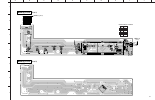
A b c d e f g h i j 1 2 3 4 5 6 7 cdc-697 31 main (1) (cb304) open/close playxchange play/pause stop 1 16 17 32 33 48 49 64 key1 key0 ext2 vccd5+5 rem /blk cl flgnd fl2 psw led ext1 flgnd vccd+5 ce di -vp fl1 vccd+5 psw key0 flgnd main (3) (cb306) main (4) p.C.B. (side a) main (4) p.C.B. (side b) • ...
2 a b c d e f g h i j 1 3 4 5 7 cdc-697 6 32 main (8) p.C.B. (side a) main (7) p.C.B. (side a) u, c, a, b, g models u, c, a, b, g models r, l models r, t, l models /pdn d4gnd -vb -vb1 fl1 fl2 main (1) (cb410) ac in ac in main (5) (cb200) main (2) (w204b) main (2) (w203b) main (2) (w205b) main (2) (w...
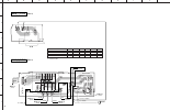
A b c d e f g h i j 1 2 3 4 5 6 7 cdc-697 33 cm (1) p.C.B. (side a) cm (2) p.C.B. (side a) cm (3) p.C.B. (side a) cm (4) p.C.B. (side a) main (1) (cb300) tbl_pos down_sw opsw close cl_down tbl_l +5 -b gnd upsw cl_sw open cl_up tbl_r gd +b 1 10 1 10 table sensor clamp up/down sw loading sw tray rotat...
Cdc-697 34 memo memo memo memo.
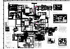
A 1 2 3 4 5 6 7 8 9 10 b c d e f g h i j k l m n cdc-697 schematic diagrams 35 ★ all voltages are measured with a 10mΩ/v dc electronic voltmeter. ★ components having special characteristics are marked s and must be replaced with parts having specifications equal to those originally installed. ★ sche...
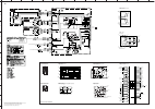
A 1 2 3 4 5 6 7 8 9 10 b c d e f g h i j k l m n cdc-697 36 ★ all voltages are measured with a 10mΩ/v dc electronic voltmeter. ★ components having special characteristics are marked s and must be replaced with parts having specifications equal to those originally installed. ★ schematic diagram is su...
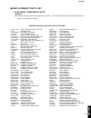
37 cdc-697 cdc-697 ■ replacement parts list abbreviations in this list are as follows: c.A.El.Chp : chip alumi.Electrolytic cap c.Ce : ceramic cap c.Ce.Array : ceramic cap array c.Ce.Chp : chip ceramic cap c.Ce.Ml : multilayer ceramic cap c.Ce.M.Chp : chip multilayer ceramic cap c.Ce.Safty : recogni...
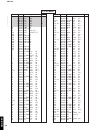
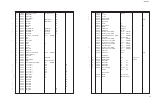
38 cdc-697 cdc-697 ✻ new parts p.C.B. Main ref. No. Part no. Description markets ✻ new parts ref. No. Part no. Description markets * wh461400 p.C.B. Main uc * wh461500 p.C.B. Main r * wh461700 p.C.B. Main t * wh461600 p.C.B. Main a * wh461800 p.C.B. Main bg * wh461900 p.C.B. Main l cb1 v2731000 cn.F...
39 cdc-697 cdc-697 ✻ new parts ref. No. Part no. Description markets ✻ new parts ref. No. Part no. Description markets p.C.B. Main and p.C.B. Cm d212 vg437700 diode.Zenr mtzj5.6b 5.6v d214 vg443300 diode.Zenr mtzj30b 30v d217 vs997800 diode 1t2 d308 v2598200 led sir‑505st d309‑312 vg437700 diode.Zen...
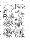
A b c d e 1 2 3 4 5 6 7 40 cdc-697 • overall ass’y cm-230a unit pu unit ass'y 203 10 22 62 202 r, l models (2) 10 (7) 22 r, t, l models 40 64 10 66 81 10 65 56 76 82 29 (1) 10 (6) (8) 62 76 22 62 62 13 36 63 72 72 65 65 6-3 6-1 6-5 6-2 6-4 6-10 65 55 5-10 5-9 67 28 23 62 61 61 200 5-3 200-1 5-10 72 ...
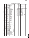
Cdc-697 41 3‑2 mf118200 flexible flat cable 18p 200mm p=1.25 * 3‑11 wh256600 front panel bl * 3‑11 wh256700 front panel ti * 3‑12 wh267500 sheet window 3‑13 v6876100 button d5 power on/off bl 3‑13 v8540300 button d5 power on/off ti * 3‑14 wh257300 sub panel bl * 3‑14 wh257400 sub panel ti 3‑16 v6034...
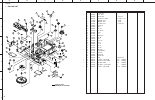
A b c d e f g h 1 2 3 4 5 6 cdc-697 42 ✻ new parts ref. No. Part no. Description remarks markets • cm-230a unit : apply the grease g31kb (part no. Vq472900) (3) 26 30 27 14 15 25 30 10 29 16 28 30 24 30 13 23 34 16 30 28 1 3 32 31 1 7 1 8 31 2 29 14 15 22 30 1 33 30 30 34 30 13 11 12 17 20 14 29 18 ...
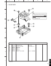
A b c d e 1 2 3 4 5 6 7 43 cdc-697 cdc-697 pu unit ass'y * 1 wh611000 pu mechanism unit da11t3cnf * 2 wh538800 flexible flat cable 16p 230mm p=1.0 10 v2430600 holder pu/c 11 v2430800 damper cdc 12 vq386500 spring 13 v2480800 barrier pu * 20 wh292300 pw head p‑tight screw 2.6x8‑12 mfzn2w3 ref. No. Pa...
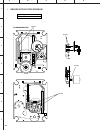
A b c d e 1 2 3 4 5 6 7 44 cdc-697 • grease application diagram pg-663 pg-663 pg-663 pu mechanism unit pg-663 apply the grease molykote pg-663 (part no. Aax01170).
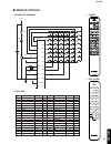
45 cdc-697 cdc-697 • panels • key code 1 2 3 4 8 9 10 11 12 13 14 15 16 17 18 19 20 21 22 23 24 25 26 27 28 29 30 31 32 33 34 35 36 37 6 7 1 2 3 4 8 9 10 11 12 13 14 15 16 17 18 19 20 21 22 23 24 25 26 27 28 29 30 31 32 33 34 35 36 37 6 7 ■ remote control • schematic diagram r2 c2 c3 15pf 15pf x1 4m...
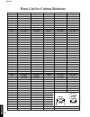
46 cdc-697 cdc-697 10mm hj35 1/4w type 5mm hf85 1/6w type hf45 1/4w type value 1/4w type part no. 1/6w type part no. 10 k Ω hf45 7100 hf45 7100 11 k Ω hf45 7110 hf45 7110 12 k Ω hj35 7120 hf85 7120 13 k Ω hf45 7130 hf45 7130 15 k Ω hf45 7150 hf45 7150 18 k Ω hf45 7180 hf45 7180 22 k Ω hf45 7220 hf45...

