Service manual important notice this manual has been provided for the use of authorized yamaha retailers and their service personnel. It has been assumed that basic service procedures inherent to the industry, and more specifically yamaha products, are already known and understood by the users, and ...
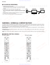
1 dsp-a595 ■ to service personnel 1. Critical components information. Components having special characteristics are marked and must be replaced with parts having specifications equal to those originally installed. 2. Leakage current measurement (for 120v model only). When service has been completed,...
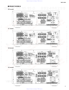
2 dsp-a595 ▼ t model ▼ b model ▼ g model ▼ r model ■ rear panels www. Xiaoyu163. Com qq 376315150 9 9 2 8 9 4 2 9 8 tel 13942296513 9 9 2 8 9 4 2 9 8 0 5 1 5 1 3 6 7 3 q q tel 13942296513 qq 376315150 892498299 tel 13942296513 qq 376315150 892498299 http://www.Xiaoyu163.Com http://www.Xiaoyu163.Com.
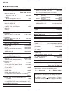
3 dsp-a595 ■ specifications ■ audio section minimum rms output power per channel (power amp. Section) main l/r, rear l/r 20hz to 20khz, 0.04% thd, 8 Ω 65w+65w 1khz, 0.07% thd, 8 Ω 80w+80w center 20hz to 20khz, 0.04% thd, 8 Ω 65w 1khz, 0.07% thd, 8 Ω 80w maximum power (eiaj) r, t models only main l/r...
4 dsp-a595 ● dimensions units: mm (inch) 21.5 (7/8") 435(17-1/8") 349.5(13-3/4") 391(15-3/8") 130(5-3/32") 151(5-15/16") 20 (13/16") 21 (27/32") warning do not change the impedance selector switch setting while the power to this unit is on, otherwise this unit may be damaged. Impedance selector www....
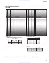
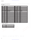
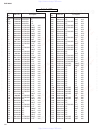
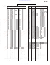
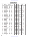
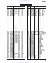
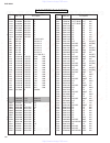
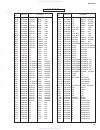
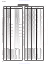
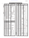
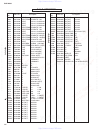
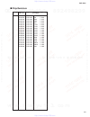
Dsp-a595 parts list for carbon resistors 160 Ω 180 Ω 200 Ω 220 Ω 270 Ω 330 Ω 390 Ω 430 Ω 470 Ω 510 Ω 560 Ω 680 Ω 820 Ω 910 Ω 1.0 k Ω 1.2 k Ω 1.5 k Ω 1.8 k Ω 2.0 k Ω 2.2 k Ω 2.4 k Ω 2.7 k Ω 3.0 k Ω 3.3 k Ω 3.6 k Ω 3.9 k Ω 4.7 k Ω 5.1 k Ω 5.6 k Ω 6.8 k Ω 8.2 k Ω 9.1 k Ω 1.0 Ω 1.8 Ω 2.2 Ω 3.3 Ω 4.7 Ω 5...
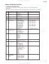
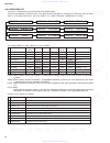
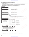
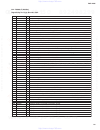
6 dsp-a595 ■ self diagnosis function 1. Purpose and operation the dsp-a595 has a self diagnosis function to locate a faulty part, if any, by inspecting and taking measurements. There are 11 main items in the diagnostic menu and some of them have sub-menu items as listed below. No. 1 2 3 4 5 6 7 8 9 ...
7 dsp-a595 1. 2. 3. 4. 5. 6. 7. Effect level : muting : off input (video) : dvd/ld (dvd/ld) center speaker : large rear speaker : large main speaker : large lfe/bass out : swfr channel center r sur l sur swfr level (db) 0 0 0 0 c. Start-up display the information of the protection function appears o...
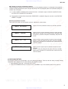
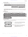
8 dsp-a595 ● history of protection function each case of the history of the protection function is displayed as shown below. Appears when the protection function has not been activated. Appears when the current protection function has been activated. When power is turned on in an abnormal status, th...
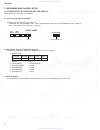
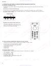
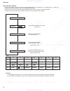
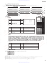
9 dsp-a595 ● selection by using the remote control unit the remote control codes in the menu list (on page 6) correspond to the dsp program, test and effect keys. See the figure on the right. 3. Operation and display when starting diagnosis function (1) selection of diagnostic menu the diagnostic me...
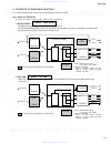
10 dsp-a595 4. Contents of diagnosis function this section describes the contents of the self diagnosis function in detail. No.1 analog through the input is fixed to analog (a/d). There are two submenus. 1. Main bypass the main l/r signals bypass the analog circuits to be output. For center/subwoofe...
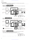
11 dsp-a595 no.2 dsp through the input is automatically discriminated by signal detection and switched with priorities ac3>pcm audio>analog. There are the following three submenus. 1. Yss908-sram main l/r are input to the dsp via ac3dav, pass through sram, and are then output to all channels without...
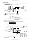
12 dsp-a595 no.3 ac3 through the input is digital signal only. Ac3 (dolby digital) decoding operation is executed, according to the input source. 1. Status(binary form) ac3 (dolby digital) decoded signals are output to each channel via ac3dav. No.4 pro logic the input is automatically discriminated ...
13 dsp-a595 no.5 speakers set the input is automatically discriminated by ac3>pcm>analog. There are the following 9 submenu items: the signal from the dsp block is normally in the effect off status for menu items 1-4. For other menu items, the same signal as in 2. Dsp through: yss908 menu is output....
14 dsp-a595 no.6 display check check program for fl display. The display status will change as follows with submenu operation. The signal is processed with effect off. All segments are turned on and off to detect defects in the fl driver and fl display segments. Then the fl driver operation is check...
15 dsp-a595 no.9 ad data check the a/d conversion values of the main cpu which detects key scan, protection, etc. Are displayed in % (100%: 5v). All signal processing before this menu is executed will be held. The keys on the main unit cannot be operated to detect the values of all keys in the k1/k2...
16 dsp-a595 no.10 status from dsp micom the status data from the dsp microprocessor is sequentially displayed in a hexadecimal number. All signal processing before this menu is executed will be held. [status 0] acmod: if it is 1000b or more with dts 7.1 signal, the dsp block will be muted. [note] al...
17 dsp-a595 11 dvd/ld s-ver:z08b main microprocessor check sum dsp microprocessor check sum main microprocessor version dsp microprocessor version one suffix letter is for compatibility of communications between the main and dsp microprocessors. * use microprocessors with the same suffix. Exit ✽ 1 t...
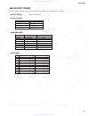
18 dsp-a595 ■ factory preset all the settings of the system are initialized on shipping. The settings are as follows. ● input (video) dvd/ld (dvd/ld) ● effect level effect channel preset value center 0 db right surround 0 db left surround 0 db sub woofer 0 db ● dsp program input dsp program delay pr...
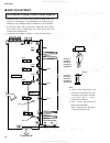
19 dsp-a595 confirmation of idling current of main amplifier • right after power is turned on, confirm that the voltage across the terminals of r688(main lch),r690(main rch), r692(center), r694(rear lch), r696(rear rch) are between 0.1mvand 5.0mv. • if it exceeds 5.0mv, open (cut off) r571 (main lch...
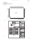
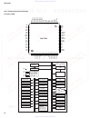
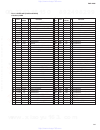
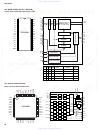
20 dsp-a595 ic800 : lc87f65c8a (lc876564a-5k19) 8 bit µ -com ■ ic data s47/pf7 s46/pf6 s45/pf5 s44/pf4 s43/pf3 s42/pf2 s41/pf1 s40/pf0 vdd4 s39/pe7 s38/pe6 s37/pe5 s36/pe4 s35/pe3 s34/pe2 s33/pe1 s32/pe0 s31/pd7 s30/pd6 s29/pd5 s19/pc3 s18/pc2 s17/pc1 s16/pc0 vdd3 s15/t15 s14/t14 s13/t13 s12/t12 s11...
21 dsp-a595 ic800 : lc87f65c8a (lc876564a-5k19) 8 bit µ -com pin pin port i/o function no. Name 1 p16 fla-clk i/o flush clock 2 p17 fla-i/o i/o flush input/output 3 p30 fla-sel i/o flush select 4 p31 t-mute o tuner mute (l: on) 5 p32 dsp-mts o transmit data for dsp 6 p33 dsp-stm i reveive data from ...
22 dsp-a595 ic800 : lc87f65c8a (lc876564a-5k19) 8 bit µ -com pin pin port i/o function no. Name 51 vp vp 52 s20/pc4 p5 o fl segment 5 53 s21/pc5 p6 o fl segment 6 54 s22/pc6 p7 o fl segment 7 55 s23/pc7 p8 o fl segment 8 56 s24/pd0 p9 o fl segment 9 57 s25/pd1 p10 o fl segment 10 58 s26/pd2 p11 o fl...
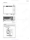
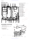
5 dsp-a595 1 2 4 5 7 8 9 0 a b d e f g h i j k c #14 #8 #7 #13 #9 3 6 ■ disassembly procedures (remove parts in disassembly order as numbered.) 1. Removal of top cover remove 4 screws ( 1 ) and 4 screws ( 2 ) in fig. 1. 2. Removal of front panel a. Remove 5 knobs. B. Remove 6 screws ( 3 ) in fig. 1....
31 32 block diagram 10 11 21 20 6ch selector ic102 26 25 27 6 5 4 8 9 7 22 23 24 operation key sw802~806, 810~815, 817,822~824 12 4 22 93 18 21 27 50 29 47 23 11 26 90 17 46 76 51 reset q803,d805 power down detect q805,d811,812 back-up (memory) q806,d813 regulator 1 2 65 65 ~ 33 12 ~ 55 40 ~ u800 tm...
20 dsp-a595 ic800 : lc87f65c8a (lc876564a-5k19) 8 bit µ -com ■ ic data s47/pf7 s46/pf6 s45/pf5 s44/pf4 s43/pf3 s42/pf2 s41/pf1 s40/pf0 vdd4 s39/pe7 s38/pe6 s37/pe5 s36/pe4 s35/pe3 s34/pe2 s33/pe1 s32/pe0 s31/pd7 s30/pd6 s29/pd5 s19/pc3 s18/pc2 s17/pc1 s16/pc0 vdd3 s15/t15 s14/t14 s13/t13 s12/t12 s11...
21 dsp-a595 ic800 : lc87f65c8a (lc876564a-5k19) 8 bit µ -com pin pin port i/o function no. Name 1 p16 fla-clk i/o flush clock 2 p17 fla-i/o i/o flush input/output 3 p30 fla-sel i/o flush select 4 p31 t-mute o tuner mute (l: on) 5 p32 dsp-mts o transmit data for dsp 6 p33 dsp-stm i reveive data from ...
22 dsp-a595 ic800 : lc87f65c8a (lc876564a-5k19) 8 bit µ -com pin pin port i/o function no. Name 51 vp vp 52 s20/pc4 p5 o fl segment 5 53 s21/pc5 p6 o fl segment 6 54 s22/pc6 p7 o fl segment 7 55 s23/pc7 p8 o fl segment 8 56 s24/pd0 p9 o fl segment 9 57 s25/pd1 p10 o fl segment 10 58 s26/pd2 p11 o fl...
23 dsp-a595 ic14 : lc87f5164a (lc875164a-5k20) 8 bit sub µ -com pb7 p07 p27/int5 p26/int5 p25/int5 p24/int5 p23/int4 p22/int4 p21/int4 p20/int4 p06 p05 p04 p03 p02 p01 p00 vss2 vdd2 pwm0 pwm1 si2p3 sck2 si2 so2 p17/pwm p16/pwl p15/sck1 p14/si1 p13/so1 p12/sck0 p11/si0 p10/soo p34 p33 p32 p31 p30 p87...
24 dsp-a595 pin pin port i/o function no. Name 1 pa3 cdo i receive data from dir2 2 pa4 /icdi o initial clear for dir2 3 pa5 /km1 o switching dir2 forced (analog) mode 4 p70/int0 lockn irq pll lock flag 5 p71/int1 errd irq dir 2 error detect 6 p72/int2 erra irq ac3dav mute detect 7 p73/int3 nonpcm i...
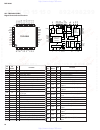
25 dsp-a595 ic3 : ym3436dk (dir2) digital format interface receiver pin pin i/o function no. Name 1 daux i auxiliary input for audio data 2 hdlt o asynchronous buffer operation flag 3 dout o audio data output 4 vfl o parity flag output 5 opt o fs x 1 synchronous output signal for dac 6 sync o fs x 1...
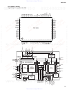
26 dsp-a595 ic4 : yss908-f (ac3dav) digital dolby pro logic decoder +dsp pvss ramd7 ramd6 ramd5 ramd4 ramd3 ramd2 ramd1 ramd0 pvdd rama2 sck si so /cs /csb rama3 test /ic rama4 pvss sdwck1 sdbck1 sdob0 sdob1 sdob2 rama7 rama8 rama9 vdd vss oport7 oport6 oport5 oport4 oport3 oport2 oport1 oport0 pvdd...
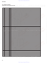
27 dsp-a595 no. Name i/o function 1 pvdd +5v power supply 2 ramcen o ram chip enable output terminal, connected to external 1m sram chip enable 3 rama16 o ram address output terminal 16, connected to external 1m sram address 4 rama15 o ram address output terminal 15, connected to external 1m sram ad...
28 dsp-a595 51 vdd +3v power supply 52 ac3data o ac-3 data output terminal, ac-3 bit stream data detect 53 crc o crc output terminal (normally unconnected) 54 mute o mute output terminal, output data mute detect 55 karaoke o karaoke output terminal, ac-3 karaoke data detect 56 surenc o surround enco...
29 dsp-a595 ic5 : m5m51288bkj-20ltel (1m sram) 131072-word x 8 bit high speed static ram nc a3 a4 a5 a6 a7 a8 a9 a10 a11 a12 a13 d1 d2 d3 gnd 1 2 3 4 5 6 7 8 9 10 11 12 13 14 15 16 vcc a2 ce2 /we a1 a0 a16 a15 /oe a14 /ce1 d8 d7 d6 d5 d4 32 31 30 29 28 27 26 25 24 23 22 21 20 19 18 17 row input buff...
30 dsp-a595 ■ display data ● v800 : 16-bt-59gk (v2421800) • grid assignment • pin connection • anode connection y 1 pattern area 18 p16 17 p17 16 p18 15 p19 14 p20 13 p21 12 p22 11 nc 10 nc 9 nc 8 nc 7 nc 6 nc 5 nc 4 np 3 np 2 f1 1 f1 pin no. Connection 19 p15 20 p14 21 p13 22 p12 23 p11 24 p10 25 p...
A 1 2 3 4 5 6 7 8 9 10 ★ all voltages are measured with a 10m Ω /v dc electric volt meter. ★ components having special characteristics are marked a n d m u s t b e r e p l a c e d w i t h p a r t s h a v i n g specifications equal to those originally installed. ★ schematic diagram is subject to chan...
H 47 b a c d e f g 1 2 3 4 5 6 dsp-a595 ■ schematic diagram (input) 48 ★ all voltages are measured with a 10m Ω /v dc electric volt meter. ★ components having special characteristics are marked and must be replaced with parts having specifications equal to those originally installed. ★ schematic dia...
A 1 2 3 4 5 6 7 8 9 10 ★ all voltages are measured with a 10m Ω /v dc electric volt meter. ★ components having special characteristics are marked a n d m u s t b e r e p l a c e d w i t h p a r t s h a v i n g specifications equal to those originally installed. ★ schematic diagram is subject to chan...
A 1 2 3 4 5 6 7 8 9 10 ★ all voltages are measured with a 10m Ω /v dc electric volt meter. ★ components having special characteristics are marked a n d m u s t b e r e p l a c e d w i t h p a r t s h a v i n g specifications equal to those originally installed. ★ schematic diagram is subject to chan...
A 1 2 3 4 5 6 7 8 9 10 ★ all voltages are measured with a 10m Ω /v dc electric volt meter. ★ components having special characteristics are marked a n d m u s t b e r e p l a c e d w i t h p a r t s h a v i n g specifications equal to those originally installed. ★ schematic diagram is subject to chan...
R r br ar al bl l l e r r re re l l le le r r br ar al bl l l e w761 #16 #16 w701 r r re re l l le le w503 w504 #14 #14 w803 phones output main l b a speakers on off b, g models only b, g models only b, g only b, g models only b, g only b, g models only r speakers +– – + main l r a b c707 c703 red b...
41 42 b a c d e f g 1 2 3 4 5 6 ■ printed circuit board (foil side) p. C. B. Main (6) dsp-a595 p. C. B. Main ( 3 ) p. C. B. Main (4) p. C. B. Main (7) p. C. B. Main (8) h ● semiconductor location ref. No. D501 d502 d503 d721 d722 d751 d762 d763 ic722 ic723 ic724 location e4 d3 e3 g3 g3 a4 c3 c2 g3 g...
H 35 b a c d e f g 1 2 3 4 5 6 dsp-a595 ■ printed circuit board (foil side) 36 p. C. B. Operation (4) p. C. B. Operation (1) p. C. B. Operation (2) ● semiconductor location ref. No. D800 d801 d802 d803 d805 d806 d807 d808 d809 d811 d812 d813 ic800 ic801 ic802 q800 q801 q802 q803 q805 q806 q810 q811 ...
37 b a c d e f h g 1 2 3 4 5 6 ■ printed circuit board (foil side) 38 dsp-a595 • r and t models p. C. B. Operation (3) • b and g models p. C. B. Operation (3) • r and t models only p. C. B. Operation (7) p. C. B. Operation (5) p. C. B. Operation (6) ref. No. Location d814 c3 d815 a2 d816 a2 q807 a2 ...
33 34 b a c d e f h g 1 2 3 4 5 6 dsp-a595 ■ printed circuit board (foil side) p. C. B. Dsp p. C. B. Dsp ref. No. Location d1 f3 d2 f3 d3 g4 d4 g4 d5 g4 d6 g4 d7 g4 d8 g4 d9 f4 d10 g4 d11 g4 d12 g4 d13 d4 d14 d4 d15 d4 d16 d4 d17 d4 ● semiconductor location ref. No. Location ic1 b3 ic2 e3 ic3 b4 ic4...
H 43 b a c d e f g 1 2 3 4 5 6 dsp-a595 ■ printed circuit board (foil side) 44 p. C. B. Input (1) ● semiconductor location ref. No. D101 d102 d103 d104 ic101 ic102 ic103 ic104 ic106 ic107 ic108 ic109 ic110 ic111 ic112 ic113 q101 location e2 e3 e2 e3 f4 f4 e4 g2 e2 d3 e4 e4 c3 d3 c4 d4 f4 b, g only a...
45 b a c d e f h g 1 2 3 4 5 6 ■ printed circuit board (foil side) 46 dsp-a595 p. C. B. Input (2) p. C. B. Input (4) p. C. B. Input (3) ● semiconductor location ref. No. D351 d352 d401 ic301 ic302 ic303 ic351 ic352 ic401 ic402 ic403 ic404 location d3 d3 f4 b3 b4 b3 d3 d4 g3 f3 f3 f4 ref. No. Q301 q3...
53 dsp-a595 parts list ■ electrical parts abbreviations in this list are as follows: c. A. El. Chp : chip alumi. Electrolytic cap c. Ce : ceramic cap c. Ce. Array : ceramic cap array c. Ce. Chp : chip ceramic cap c. Ce. Ml : multilayer ceramic cap c. Ce. M. Chp : chip multilayer ceramic cap c. Ce. S...
54 dsp-a595 p. C. B. Dsp schm ref part no. Description ✻ new parts ✻ new parts schm ref part no. Description v3005700 p.C.B. Dsp cb1 vq044200 cn.Bs.Pin 6p cb3 vq044500 cn.Bs.Pin 11p cb6 vq044600 cn.Bs.Pin 13p c1 ub245100 c.Ce.M.Chp 0.1uf 25v c2 ub052100 c.Ce.M.Chp 100pf 50v c3 ub052100 c.Ce.M.Chp 10...
55 dsp-a595 schm ref part no. Description ✻ new parts ✻ new parts schm ref part no. Description p. C. B. Dsp & p. C. B. Input c120 ur847100 c.El 10uf 25v c121 ur847100 c.El 10uf 25v c122 ua952100 c.Mylar 100pf 50v c123 ur837220 c.El 22uf 25v c124 ur847100 c.El 10uf 25v c125 ur837220 c.El 22uf 25v c1...
56 dsp-a595 p. C. B. Input schm ref part no. Description ✻ new parts ✻ new parts schm ref part no. Description c101 ur866220 c.El 2.2uf 50v c102 ua952100 c.Mylar 100pf 50v(bg) c103 ua952220 c.Mylar 220pf 50v c104 ua952100 c.Mylar 100pf 50v(bg) c105 ua952220 c.Mylar 220pf 50v c106 ur866220 c.El 2.2uf...
57 dsp-a595 p. C. B. Input schm ref part no. Description ✻ new parts ✻ new parts schm ref part no. Description c311 vf466800 c.Ce.Tublr 100pf 50v c312 vf467000 c.Ce.Tublr 1000pf 50v c313 ur837100 c.El 10uf 16v c314 vf466800 c.Ce.Tublr 100pf 50v c315 ur837330 c.El 33uf 16v c316 vg276600 c.Ce.Tublr 22...
58 dsp-a595 p. C. B. Input & p. C. B. Main schm ref part no. Description ✻ new parts ✻ new parts schm ref part no. Description pj101 vq260900 jack.Pin 4p pj102 vv306900 jack.Pin 4p pj103 vv306900 jack.Pin 4p pj104 vu857800 jack.Pin 6p pj105 vk437600 jack.Pin 1p pj301 vv325000 jack.Pin 2p pj302 vv852...
59 dsp-a595 p. C. B. Main schm ref part no. Description ✻ new parts ✻ new parts schm ref part no. Description c547 ur867470 c.El 47uf 50v c548 vq645600 c.Mylar 100pf 50v c549 vr325000 c.Mylar 100pf 100v c550 ur867470 c.El 47uf 50v c551 vr325000 c.Mylar 100pf 100v c552 vr325000 c.Mylar 100pf 100v c55...
60 dsp-a595 p. C. B. Main schm ref part no. Description ✻ new parts ✻ new parts schm ref part no. Description q511 vp883000 tr 2sa893a d,e q512 vr325600 tr 2sc2229 o,y q513 vp883000 tr 2sa893a d,e q514 vr325600 tr 2sc2229 o,y q515 vp883000 tr 2sa893a d,e q516 vr325600 tr 2sc2229 o,y q517 vp883000 tr...
61 dsp-a595 schm ref part no. Description ✻ new parts ✻ new parts schm ref part no. Description p. C. B. Main & p. C. B. Operation r690 hz003780 r.Mtl.Plat 0.22 Ω +0.22 5w r692 vu981700 r.Mtl.Plat 0.22 Ω +0.22 3w r694 vu981700 r.Mtl.Plat 0.22 Ω +0.22 3w r696 vu981700 r.Mtl.Plat 0.22 Ω +0.22 3w r711 ...
62 dsp-a595 schm ref part no. Description ✻ new parts ✻ new parts schm ref part no. Description p. C. B. Operation d801 vd631600 diode 1ss133,176,hss104 d802 vm974100 diode.Zenr hzs5b2td 5.0v d803 vd631600 diode 1ss133,176,hss104 d805 vd631600 diode 1ss133,176,hss104 d806 vd631600 diode 1ss133,176,h...
63 dsp-a595 ✻ new parts schm ref part no. Description ■ chip resistors rd250000 r.Car.Chp 0 Ω 1/10w rd254470 r.Car.Chp 47 Ω 1/10w rd255100 r.Car.Chp 100 Ω 1/10w rd255330 r.Car.Chp 330 Ω 1/10w rd256100 r.Car.Chp 1k Ω 1/10w rd256120 r.Car.Chp 1.2k Ω 1/10w rd256150 r.Car.Chp 1.5k Ω 1/10w rd256220 r.Car...
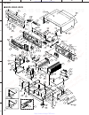
64 dsp-a595 b a c d 1 2 3 4 5 6 ■ exploded view b model g model jk ass'y vr ass'y sw ass'y vr ass'y (5) (4) (4) (2) (6) (4) (7) (7) (8) (2) (1) (3) (3) (6) (3) (2) (1) (5) (1) (r,t only) (b,g only) (r,t only) (g only) (g only) 1-4 162 3-2 2-1 124 1-1 2-1 2-23 2-24 2-23 2-8 25 30 8 17 16 176 160 160 ...
Dsp-a595 ref. No. Part no. Description remarks markets ✻ new parts ref. No. Part no. Description remarks markets ✻ new parts 65 66 ■ mechanical parts 1- 1 v2464300 front panel bl 1- 1 v2464400 front panel ti 1- 4 v2468600 escutchoen 3/8 2- 1 v3005400 p.C.B. Ass’y operation (rt) 2- 1 v3005500 p.C.B. ...

